1. Introduction
1.1. Operational Amplifiers (op amp)
The name of operational amplifier found its name due to its performance in mathematical operations (addition, subtraction, integration and differentiation)
| [1] | R. Jacob Baker, Harry W. Li and David E. Boyce, CMOS Circuit Design, Layout, and Simulation, IEEE Press, 3rd Edition, (1998). |
| [2] | Amana Yadav, Jane (2012) a Review Paper on Design and Synthesis of Two Stage CMOS Op-Amp, Ijaet ISSN: 2231-1963677, 2, Issue 1, pp. 677-688. |
[1, 2]
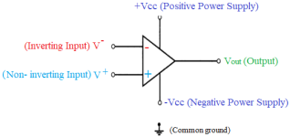
. It is a five-terminal device as shown in the
figure 1 below
| [3] | Behzad Razavi, Design of Analog CMOS Integrated Circuits, McGraw-Hill Higher education, New York, 2001. |
[3]
.
Op-amp is very large gain material which amplifies the difference of its two input voltages
| [4] | Paul R. Gray, Stephen H. Lewis, Robert G. Meyer And Paul J. Hurst, Analysis and Design Of Analog Integrated Circuits, Fifth Edition, (2001). |
[4]
. If input is applied to the non-inverting terminal, we will get amplified output with the same polarity with input
| [6] | LiTi anwang, Ye Bo, and Jiang Jingnang, “A Novel Fully Differential Telescopic Operational Transconductance Amplifier” Journal of semiconductors, 30, No. 8 August 2009. |
[6]
. Whereas if we apply the input to the inverting terminal will get amplified but inverted output
| [5] | Johan H. Huijsing (2001), Operational amplifiers-theory and design, Kluwer Academic Publishers, Boston, USA. |
| [6] | LiTi anwang, Ye Bo, and Jiang Jingnang, “A Novel Fully Differential Telescopic Operational Transconductance Amplifier” Journal of semiconductors, 30, No. 8 August 2009. |
| [7] | JAMES K. ROBERGE, (1976), Operational Amplifiers Theory and Practice, Massachusetts Institute of Technology, New York. |
[5-7]
. Op-amps are electronic devices which are mostly today
| [8] | Philip E. Allen and Douglas R. Holberg (2002), CMOS Analog Circuit Design, 2nd Edition, Oxford University Press, New York. |
[8]
. Such as: used in a wide array of consumer, industrial, medical and scientific devices, etc.
| [8] | Philip E. Allen and Douglas R. Holberg (2002), CMOS Analog Circuit Design, 2nd Edition, Oxford University Press, New York. |
[8]
.
1.2. Performance Parameters of op-amp
To designing op-amp we must consider many important performance parameters, which indicate quality of op-amp
| [5] | Johan H. Huijsing (2001), Operational amplifiers-theory and design, Kluwer Academic Publishers, Boston, USA. |
[5]
. The following are the main performance parameters that indicate the efficiency of op-amp.
Open loop Voltage gain (
): it is obtained by taking the ratio of the output voltage
to differential input voltage
within open loop circuit
| [5] | Johan H. Huijsing (2001), Operational amplifiers-theory and design, Kluwer Academic Publishers, Boston, USA. |
[5]
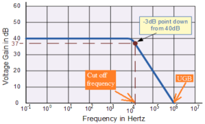
. The open loop gain of an operational amplifier is not varying at very small frequency; however it decreases very fast with exceeding frequency see
figure 2 | [9] | ALAN B. Grebene, (1983), Bipolar and MOS Analog Integrated Circuit Design, Micro-Linear Corporation Sunnyvale, California. |
[9]
.
The unity-gain frequency (UGB): Is the value of frequency at where gain reduces to zero dB or unity
| [10] | Achala Shukla1, Ankur Girolkar1, Jagveer Verma, Review of Folded Cascode & Telescopic Op-Amp, Thesis Desrtaion, 4, Issue 05, May 2017. |
[10]
.
Common Mode Rejection Ratio (CMRR): It is obtained by taking the ratio of magnitude of differential voltage gain to the common mode gain
| [7] | JAMES K. ROBERGE, (1976), Operational Amplifiers Theory and Practice, Massachusetts Institute of Technology, New York. |
[7]
. It shows that strength of an op-amp to reject noise, and magnifies any signals that are differential between them
| [7] | JAMES K. ROBERGE, (1976), Operational Amplifiers Theory and Practice, Massachusetts Institute of Technology, New York. |
[7]
.
Input common mode range: It is the very large range of the common-mode input voltage which does not generate a significant difference on differential gain
| [3] | Behzad Razavi, Design of Analog CMOS Integrated Circuits, McGraw-Hill Higher education, New York, 2001. |
[3]
.
Phase margin (PM): It indicates the phase shift of the amplifier at the unit gain bandwidth
| [8] | Philip E. Allen and Douglas R. Holberg (2002), CMOS Analog Circuit Design, 2nd Edition, Oxford University Press, New York. |
[8]
. Therefore, it measures the stability of op amp
| [1] | R. Jacob Baker, Harry W. Li and David E. Boyce, CMOS Circuit Design, Layout, and Simulation, IEEE Press, 3rd Edition, (1998). |
| [8] | Philip E. Allen and Douglas R. Holberg (2002), CMOS Analog Circuit Design, 2nd Edition, Oxford University Press, New York. |
[1, 8]
.
Output voltage swing: It is the maximum output voltage that the op-amp can produce before clipping for certain load and working applied voltage
| [11] | Stout, D. F. (1976). Handbook of Operational Amplifier Circuit Design. McGraw-Hill. pp. 1–11. ISBN 0-07-061797-X. |
[11]
.
Slew Rate (SR): Is the ratio of output voltage for a step-signal input to time
| [7] | JAMES K. ROBERGE, (1976), Operational Amplifiers Theory and Practice, Massachusetts Institute of Technology, New York. |
[7]
. Therefore, in other words it is the measure of the slope of the output voltage
| [7] | JAMES K. ROBERGE, (1976), Operational Amplifiers Theory and Practice, Massachusetts Institute of Technology, New York. |
[7]
.
Mathematically it is given by:
Unit of slew rate is V/µs
| [8] | Philip E. Allen and Douglas R. Holberg (2002), CMOS Analog Circuit Design, 2nd Edition, Oxford University Press, New York. |
[8]
. For ideal op-amp slew rate is infinity
| [7] | JAMES K. ROBERGE, (1976), Operational Amplifiers Theory and Practice, Massachusetts Institute of Technology, New York. |
[7]
. The output reaches at the same instant of input application
| [7] | JAMES K. ROBERGE, (1976), Operational Amplifiers Theory and Practice, Massachusetts Institute of Technology, New York. |
[7]
. This shows that the input reaches to the output without losing of time
| [9] | ALAN B. Grebene, (1983), Bipolar and MOS Analog Integrated Circuit Design, Micro-Linear Corporation Sunnyvale, California. |
[9]
. We can get largest slew rates in op-amps by using high frequencies
| [9] | ALAN B. Grebene, (1983), Bipolar and MOS Analog Integrated Circuit Design, Micro-Linear Corporation Sunnyvale, California. |
[9]
.
Total power dissipation (PD): Is the power used by the device
| [8] | Philip E. Allen and Douglas R. Holberg (2002), CMOS Analog Circuit Design, 2nd Edition, Oxford University Press, New York. |
[8]
. Ideally op amp does not use any power. However practical op amp dissipates finite power
| [9] | ALAN B. Grebene, (1983), Bipolar and MOS Analog Integrated Circuit Design, Micro-Linear Corporation Sunnyvale, California. |
[9]
. If the power used by the device is low, then it can operate for long time
| [7] | JAMES K. ROBERGE, (1976), Operational Amplifiers Theory and Practice, Massachusetts Institute of Technology, New York. |
| [8] | Philip E. Allen and Douglas R. Holberg (2002), CMOS Analog Circuit Design, 2nd Edition, Oxford University Press, New York. |
| [9] | ALAN B. Grebene, (1983), Bipolar and MOS Analog Integrated Circuit Design, Micro-Linear Corporation Sunnyvale, California. |
[7-9]
. The lower the power dissipation the better the device is
| [9] | ALAN B. Grebene, (1983), Bipolar and MOS Analog Integrated Circuit Design, Micro-Linear Corporation Sunnyvale, California. |
[9]
.
1.3. Types of CMOS Operational Amplifier Topologies
We can classify op-amp topologies in to four. These are single stage op-amp, two stage op-amp, Folded- cascode op-amp, and Telescopic op-amp
| [12] | Wikipedia. Operational amplifier. Available from: https://en.wikipedia.org/wiki/Operational_amplifier (accessed 30 April 2024) |
| [13] | David Terrell, (1996). OP AMPS Design Application and Troubleshooting, 2nd Edition. |
| [14] | Whites, EE 320, (2016). Lecture 25: Enhancement Type MOSFET Operation, P channel, N-channel and CMOS. |
| [15] | Wikipedia. MOSFET. Available from: https://simple.wikipedia.org/wiki/MOSFET#Referencs (accessed 23 August 2023) |
| [16] | Dara Rama Krishna and Dr. R. V. S. Satyanarayana, Design of Telescopic Cascode Single Stage Operational Transconductance Amplifier, Asian Journal Of Science And Technology, 09, Issue, 03, PP. 7737-7739, March, 2018. |
[12-16]
.
Single stage CMOS operational amplifier
Single stage CMOS op-amp has small size to design as shown in the
figure 3 . It has small gain due to its small output impedance
| [14] | Whites, EE 320, (2016). Lecture 25: Enhancement Type MOSFET Operation, P channel, N-channel and CMOS. |
| [15] | Wikipedia. MOSFET. Available from: https://simple.wikipedia.org/wiki/MOSFET#Referencs (accessed 23 August 2023) |
| [16] | Dara Rama Krishna and Dr. R. V. S. Satyanarayana, Design of Telescopic Cascode Single Stage Operational Transconductance Amplifier, Asian Journal Of Science And Technology, 09, Issue, 03, PP. 7737-7739, March, 2018. |
| [17] | E. Srinivas, N. Balaji and L. Padma Sree, A Novel Methodology of Simulation and Realization of Various Op amp Topologies In 0.18µm CMOS technology using matlab, International Journal Of VLSI Design & Communication Systems (VLSICS), 6, No. 5, October 2015. |
| [18] | Nirav Desai, Ramesh Harjani, Design Of An Operation Amplifier For Switched Capacitor Filter Application With 50 MHZ Unity Gain Bandwidth and 42.5db Gain, IOSR Journal Of VLSI And Signal Processing (IOSR-JVSP) 6, Issue 3, Ver. I (May-Jun. 2016), PP 82-88 E-ISSN: 2319 – 4200, P-ISSN No. 2319–4197 www.Iosrjournals.Org |
| [19] | K. Gulati, H. Si Lee “A ±2.45V-swing CMOS Telescopic Operational Amplifier” Massachusetts Institute of Technology, Cambridge, MA. |
| [20] | J. Mallek, H. Mnif, H. Daoud, and M. Loulou “A Fully-differential Regulated Telescopic Operational Transconducatnce Amplifier “Recent Advances in Electrical and Computer Engineering ISBN: 978-1-61804-228-6. |
| [21] | Falk Roewer and Ulrich Kleine, “A Novel class of complementary folded-cascode op amps for low voltage”, IEEE Journal of Solid State Circuits, Vol. 37, no. 8, August 2002. |
| [22] | Er. Rajni, “Design of High Gain Folded-Cascode Operational Amplifier Using 1.25 um CMOS Technology”, International Journal of Scientific & Engineering Research Volume 2, Issue 11, November-2011. |
| [23] | Ratnaprabha w. Jasutkar, P. R. Bajaj & A. Y. Deshmukh, “Design of 1v, 0.18μ Folded cascode operational amplifier for switch Capacitor sigma delta modulator”, International Journal of Electrical and Electronics Engineering Research (IJEEER) Vol. 3, Issue 4, Oct 2013. |
| [24] | Jalpa solanki, “Design and Implementation of High Gain, High Bandwidth CMOS Folded cascode Operational Transconductance Amplifier”, 2014 IJEDR Volume 2, Issue 1 ISSN: 2321-9939. |
| [25] | B. G. Song, O. J. Kwon, I. K. Chang, H. J. SONG and K. D. Kwack, ‖A 1.8V Self-Biased Complementary Folded-Cascode Amplifier ‖, IEEE J. Solid State circuits pg. No. 63-65, 1999. |
| [26] | Zhang Kun+, Wu Di and Liu Zhangfa, “A High-performance Folded Cascode Amplifier”, International Conference on Computer and Automation Engineering (ICCAE 2011) IPCSIT vol. 44 (2012), https://doi.org/10.7763/IPCSIT.2012.V44.8 |
| [27] | Pallavi Kothe, “Design and Characterization of Low Power Folded-Cascode Operational Amplifier”, International Conference on Recent Trends in Engineering Science and Technology (ICRTEST 2017) ISSN: 2321-8169-425 – 427 Volume: 5 Issue: 1 (Special Issue 21-22 January 2017). |
| [28] | J. Mahattanakul, “Design procedure for two-stage CMOS operational amplifiers employing current buffer,” IEE transactions on circuit and systems-ii: express briefs, vol-52, No. 11, and November 2005. |
| [29] | Siti Nur Syuhadah Baharudin, Asral Bahari Jambek and Rizalafande Che Ismail “Design and Analysis of a Two-stage OTA for Sensor Interface Circuit” 2014 IEEE symposium on Computer applications & Industrial Electronics (ISCAIE 2014), April 7-8, 2014, Penang, Malaysia. |
| [30] | Mohd Haidar Hamzah, Asral Bahari Jambek, Uda Hashim “Design and Analysis of a Two-stage CMOS Op-amp using Silterra’s 0.13 um Technology” 2014 IEEE Symposium on Computer applications & Industrial Electronics (ISCAIE 2014), April 7-8, 2014, Penang, Malaysia. |
[14-30]
. But, its small output impudence leads to large unity gain bandwidth and large speed. Due to large speed it has small power dissipation
| [12] | Wikipedia. Operational amplifier. Available from: https://en.wikipedia.org/wiki/Operational_amplifier (accessed 30 April 2024) |
| [13] | David Terrell, (1996). OP AMPS Design Application and Troubleshooting, 2nd Edition. |
| [14] | Whites, EE 320, (2016). Lecture 25: Enhancement Type MOSFET Operation, P channel, N-channel and CMOS. |
| [15] | Wikipedia. MOSFET. Available from: https://simple.wikipedia.org/wiki/MOSFET#Referencs (accessed 23 August 2023) |
| [16] | Dara Rama Krishna and Dr. R. V. S. Satyanarayana, Design of Telescopic Cascode Single Stage Operational Transconductance Amplifier, Asian Journal Of Science And Technology, 09, Issue, 03, PP. 7737-7739, March, 2018. |
[12-16]
.
Single stage Telescopic cascode CMOS op-amp
Figure 4. shows topology of telescopic cascade op-amp. In order to obtain larger gain than single stage, we can use cascading (transistors are cascaded between the power supplies in series)
| [15] | Wikipedia. MOSFET. Available from: https://simple.wikipedia.org/wiki/MOSFET#Referencs (accessed 23 August 2023) |
| [16] | Dara Rama Krishna and Dr. R. V. S. Satyanarayana, Design of Telescopic Cascode Single Stage Operational Transconductance Amplifier, Asian Journal Of Science And Technology, 09, Issue, 03, PP. 7737-7739, March, 2018. |
[15, 16]
. Single stage op-amp has smaller gain than telescopic cascade op-amp
| [16] | Dara Rama Krishna and Dr. R. V. S. Satyanarayana, Design of Telescopic Cascode Single Stage Operational Transconductance Amplifier, Asian Journal Of Science And Technology, 09, Issue, 03, PP. 7737-7739, March, 2018. |
| [17] | E. Srinivas, N. Balaji and L. Padma Sree, A Novel Methodology of Simulation and Realization of Various Op amp Topologies In 0.18µm CMOS technology using matlab, International Journal Of VLSI Design & Communication Systems (VLSICS), 6, No. 5, October 2015. |
| [18] | Nirav Desai, Ramesh Harjani, Design Of An Operation Amplifier For Switched Capacitor Filter Application With 50 MHZ Unity Gain Bandwidth and 42.5db Gain, IOSR Journal Of VLSI And Signal Processing (IOSR-JVSP) 6, Issue 3, Ver. I (May-Jun. 2016), PP 82-88 E-ISSN: 2319 – 4200, P-ISSN No. 2319–4197 www.Iosrjournals.Org |
[16-18]
. Disadvantage of this topology is the very small output swing. Due to its high speed telescopic op-amp has low power dissipation
| [15] | Wikipedia. MOSFET. Available from: https://simple.wikipedia.org/wiki/MOSFET#Referencs (accessed 23 August 2023) |
| [16] | Dara Rama Krishna and Dr. R. V. S. Satyanarayana, Design of Telescopic Cascode Single Stage Operational Transconductance Amplifier, Asian Journal Of Science And Technology, 09, Issue, 03, PP. 7737-7739, March, 2018. |
| [17] | E. Srinivas, N. Balaji and L. Padma Sree, A Novel Methodology of Simulation and Realization of Various Op amp Topologies In 0.18µm CMOS technology using matlab, International Journal Of VLSI Design & Communication Systems (VLSICS), 6, No. 5, October 2015. |
| [18] | Nirav Desai, Ramesh Harjani, Design Of An Operation Amplifier For Switched Capacitor Filter Application With 50 MHZ Unity Gain Bandwidth and 42.5db Gain, IOSR Journal Of VLSI And Signal Processing (IOSR-JVSP) 6, Issue 3, Ver. I (May-Jun. 2016), PP 82-88 E-ISSN: 2319 – 4200, P-ISSN No. 2319–4197 www.Iosrjournals.Org |
| [19] | K. Gulati, H. Si Lee “A ±2.45V-swing CMOS Telescopic Operational Amplifier” Massachusetts Institute of Technology, Cambridge, MA. |
| [20] | J. Mallek, H. Mnif, H. Daoud, and M. Loulou “A Fully-differential Regulated Telescopic Operational Transconducatnce Amplifier “Recent Advances in Electrical and Computer Engineering ISBN: 978-1-61804-228-6. |
[15-20]
.
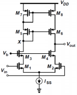
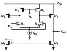
Folded cascode op-amp
In order to solve some of the disadvantages of telescopic op-amps such as limited output swing, we can use a “folded cascode” as shown
figure 5 | [21] | Falk Roewer and Ulrich Kleine, “A Novel class of complementary folded-cascode op amps for low voltage”, IEEE Journal of Solid State Circuits, Vol. 37, no. 8, August 2002. |
| [22] | Er. Rajni, “Design of High Gain Folded-Cascode Operational Amplifier Using 1.25 um CMOS Technology”, International Journal of Scientific & Engineering Research Volume 2, Issue 11, November-2011. |
| [23] | Ratnaprabha w. Jasutkar, P. R. Bajaj & A. Y. Deshmukh, “Design of 1v, 0.18μ Folded cascode operational amplifier for switch Capacitor sigma delta modulator”, International Journal of Electrical and Electronics Engineering Research (IJEEER) Vol. 3, Issue 4, Oct 2013. |
[21-23]
. This topology lies between telescopic and two stage op-amps. It has low supply input voltage
| [22] | Er. Rajni, “Design of High Gain Folded-Cascode Operational Amplifier Using 1.25 um CMOS Technology”, International Journal of Scientific & Engineering Research Volume 2, Issue 11, November-2011. |
[22]
. However due to its high output impendence, high power dissipation and low speed folded cascode op amp has larger output voltage swing
| [24] | Jalpa solanki, “Design and Implementation of High Gain, High Bandwidth CMOS Folded cascode Operational Transconductance Amplifier”, 2014 IJEDR Volume 2, Issue 1 ISSN: 2321-9939. |
[24]
. The gain of the folded cascade is smaller than the two stage op amp, but greater than telescopic
| [22] | Er. Rajni, “Design of High Gain Folded-Cascode Operational Amplifier Using 1.25 um CMOS Technology”, International Journal of Scientific & Engineering Research Volume 2, Issue 11, November-2011. |
| [23] | Ratnaprabha w. Jasutkar, P. R. Bajaj & A. Y. Deshmukh, “Design of 1v, 0.18μ Folded cascode operational amplifier for switch Capacitor sigma delta modulator”, International Journal of Electrical and Electronics Engineering Research (IJEEER) Vol. 3, Issue 4, Oct 2013. |
| [24] | Jalpa solanki, “Design and Implementation of High Gain, High Bandwidth CMOS Folded cascode Operational Transconductance Amplifier”, 2014 IJEDR Volume 2, Issue 1 ISSN: 2321-9939. |
[22-24]
. Telescopic cascade op amp has larger speed folded cascode op amp
| [21] | Falk Roewer and Ulrich Kleine, “A Novel class of complementary folded-cascode op amps for low voltage”, IEEE Journal of Solid State Circuits, Vol. 37, no. 8, August 2002. |
| [22] | Er. Rajni, “Design of High Gain Folded-Cascode Operational Amplifier Using 1.25 um CMOS Technology”, International Journal of Scientific & Engineering Research Volume 2, Issue 11, November-2011. |
| [23] | Ratnaprabha w. Jasutkar, P. R. Bajaj & A. Y. Deshmukh, “Design of 1v, 0.18μ Folded cascode operational amplifier for switch Capacitor sigma delta modulator”, International Journal of Electrical and Electronics Engineering Research (IJEEER) Vol. 3, Issue 4, Oct 2013. |
| [24] | Jalpa solanki, “Design and Implementation of High Gain, High Bandwidth CMOS Folded cascode Operational Transconductance Amplifier”, 2014 IJEDR Volume 2, Issue 1 ISSN: 2321-9939. |
[21-24]
.
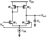
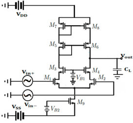
Two stage op-amp:
In order to design amplifiers with both large gain and high swing, one must apply two-stage amplifier as shown in the
figure 6 | [26] | Zhang Kun+, Wu Di and Liu Zhangfa, “A High-performance Folded Cascode Amplifier”, International Conference on Computer and Automation Engineering (ICCAE 2011) IPCSIT vol. 44 (2012), https://doi.org/10.7763/IPCSIT.2012.V44.8 |
| [27] | Pallavi Kothe, “Design and Characterization of Low Power Folded-Cascode Operational Amplifier”, International Conference on Recent Trends in Engineering Science and Technology (ICRTEST 2017) ISSN: 2321-8169-425 – 427 Volume: 5 Issue: 1 (Special Issue 21-22 January 2017). |
| [28] | J. Mahattanakul, “Design procedure for two-stage CMOS operational amplifiers employing current buffer,” IEE transactions on circuit and systems-ii: express briefs, vol-52, No. 11, and November 2005. |
[26-28]
. First stage of two stage op amp is used to produce high gain, whereas second stage produces large swing
| [27] | Pallavi Kothe, “Design and Characterization of Low Power Folded-Cascode Operational Amplifier”, International Conference on Recent Trends in Engineering Science and Technology (ICRTEST 2017) ISSN: 2321-8169-425 – 427 Volume: 5 Issue: 1 (Special Issue 21-22 January 2017). |
| [28] | J. Mahattanakul, “Design procedure for two-stage CMOS operational amplifiers employing current buffer,” IEE transactions on circuit and systems-ii: express briefs, vol-52, No. 11, and November 2005. |
| [29] | Siti Nur Syuhadah Baharudin, Asral Bahari Jambek and Rizalafande Che Ismail “Design and Analysis of a Two-stage OTA for Sensor Interface Circuit” 2014 IEEE symposium on Computer applications & Industrial Electronics (ISCAIE 2014), April 7-8, 2014, Penang, Malaysia. |
[27-29]
. But, it has compromised frequency response, large power consumption (because of two stages), and small speed and has very low power supply rejection at high frequencies
| [26] | Zhang Kun+, Wu Di and Liu Zhangfa, “A High-performance Folded Cascode Amplifier”, International Conference on Computer and Automation Engineering (ICCAE 2011) IPCSIT vol. 44 (2012), https://doi.org/10.7763/IPCSIT.2012.V44.8 |
| [27] | Pallavi Kothe, “Design and Characterization of Low Power Folded-Cascode Operational Amplifier”, International Conference on Recent Trends in Engineering Science and Technology (ICRTEST 2017) ISSN: 2321-8169-425 – 427 Volume: 5 Issue: 1 (Special Issue 21-22 January 2017). |
| [28] | J. Mahattanakul, “Design procedure for two-stage CMOS operational amplifiers employing current buffer,” IEE transactions on circuit and systems-ii: express briefs, vol-52, No. 11, and November 2005. |
| [29] | Siti Nur Syuhadah Baharudin, Asral Bahari Jambek and Rizalafande Che Ismail “Design and Analysis of a Two-stage OTA for Sensor Interface Circuit” 2014 IEEE symposium on Computer applications & Industrial Electronics (ISCAIE 2014), April 7-8, 2014, Penang, Malaysia. |
| [30] | Mohd Haidar Hamzah, Asral Bahari Jambek, Uda Hashim “Design and Analysis of a Two-stage CMOS Op-amp using Silterra’s 0.13 um Technology” 2014 IEEE Symposium on Computer applications & Industrial Electronics (ISCAIE 2014), April 7-8, 2014, Penang, Malaysia. |
[26-30]
. The larger output swing produced by the second stage is used for some applications, mostly with lower supply voltages in today’s technologies
| [10] | Achala Shukla1, Ankur Girolkar1, Jagveer Verma, Review of Folded Cascode & Telescopic Op-Amp, Thesis Desrtaion, 4, Issue 05, May 2017. |
| [17] | E. Srinivas, N. Balaji and L. Padma Sree, A Novel Methodology of Simulation and Realization of Various Op amp Topologies In 0.18µm CMOS technology using matlab, International Journal Of VLSI Design & Communication Systems (VLSICS), 6, No. 5, October 2015. |
[10, 17]
.
2. Methodology and DESIGN Techniques
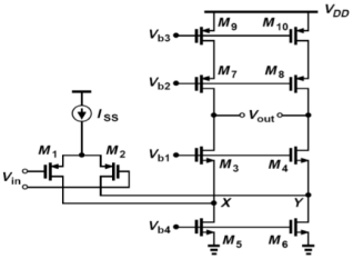
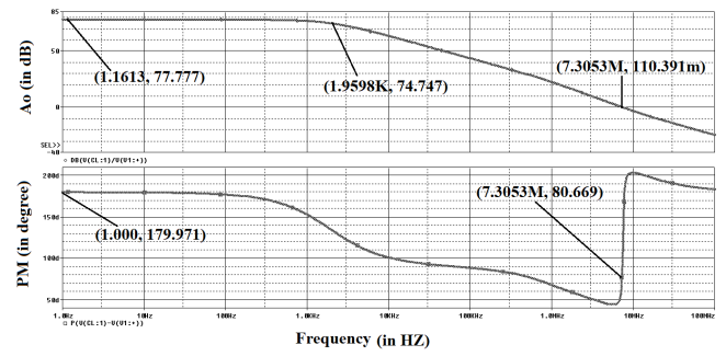
Usually there are many topologies used for a particular functionality. The designer has to choose an appropriate circuit topology which meets the specification. The topology of the circuit to be designed in this research work is a single stage telescopic CMOS op-amp, shown in
figure 7.
The circuit consists of nine transistors: out of which five (
and
) are NMOS and the remaining four
,
and
are PMOS transistors. Transistors
and
form the basic differential input stage. Since NMOS transistors give more current source and gain than PMOS transistors
| [3] | Behzad Razavi, Design of Analog CMOS Integrated Circuits, McGraw-Hill Higher education, New York, 2001. |
[3]
. That is why we choice NMOS transistors in differential input rather than PMOS transistors. The gate of
is the inverting input and the gate of
is the non-inverting input. The differential input signal applied across the two input terminals will be amplified according to the gain of the differential stage, which is simply the Transconductance of
times the total output resistance seen at the output.
The transistors and are used to convert differential input signal in to single output signal. While the transistors , and used to increase the output swing and the gain. The transistor M9 act as current source and it is expected to give more drain source current.
The gates of should be biased by a voltage that keeps it in saturation. The gates of and should be biased by a voltage that keeps both and in saturation and which, at the same time, should avoid going into triode region.
2.2. Design Specifications
Generally, the idea behind any design procedure is to get a circuit that meets certain specifications. Therefore, the single stage telescopic CMOS op-amp designed in this study is expected to meet the specifications listed in
table 1. The design of a single stage telescopic CMOS op-amp uses 1µm CMOS technology.
Table 1. List of specifications for single stage Telescopic CMOS op-amp.
Parameter | Proposed value |
Open loop gain | ≥40dB |
Load capacitance | 2pf |
UGB | ≥1MHz |
ICMR | 1.12V to 1.4V |
Supply Voltages ( | (5V, 5V) |
Power dissipation | ≤10mw |
Phase margin | ≥45º |
Table 2. List of constant parameters and boundary conditions.
Constant parameter | Value |
Tail current | ≤99µA |
Constant parameter for NMOS ( | |
Constant parameter for PMOS ( | |
Thresh hold voltage for NMOS ( | 0.65V |
Thresh hold voltage for PMOS ( | -0.65V |
Minimum length (L) | 1m |
All the transistors in the design are expected to be in saturation mode of operation. Since to use transistor as amplifier, they must be in saturation region unless output signals become distorted and nonlinear
| [8] | Philip E. Allen and Douglas R. Holberg (2002), CMOS Analog Circuit Design, 2nd Edition, Oxford University Press, New York. |
[8]
. The procedure and basic relationship that we have used in the design process are described as follows:
Step 1: we must estimate the tail current , by using definition of slew rate. i.e.:
Step 2: Design tail transistor by calculating its width (W) and length (L) by using the transistor in saturation equation. The equation used is:
(3)
In addition bias voltage of transistor is equal to its gate source voltage. i.e
Step 3: Design the differential pair of the circuit ( and ) by assuming both of them to be working in saturation mode, and the current moving through them is half of the tail current. Their aspect ratios could be calculated using the following equation.
(4)
Step 4: Design transistor ( and ) by assuming the two transistors used are identical and in saturation mode. Calculate their aspect ratios by using the following equation.
(5)
Where:
By assuming bias voltage,
Step 5: Design the Cascode Current Mirror stage (, and ) where there are four PMOS transistors by assuming the drain source current passing through them is similar to the drain and gate are tied to each other. The transistors , and will be designed by using equation 2.5 and 2.6 respectively.
(6)
Where
(7)
Where,
2.4. Mathematical Formulations
We can estimate the tail current by using equation (
2) as follow as:
From boundary condition ≤ 99 µA. by taking large current ensures all transistors to operate in saturation region. So, take tail current as 58.92µA.
Tail transistor
may be designed by using the equation
3. i.e.
Since we assume that input pair
We are taking L as 10 times the technology parameter. Thus, W and L of transistor M9 are:
We assume that VB2=0.8V
The differential pair of the circuit (
and
) may be designed by assuming both of them to be working in saturation mode, and the current flowing through them is half of the tail current. Their aspect ratios could be calculated applying equation (
4) as follow as:
We are taking L as 10 times the technology parameter. Thus, W and L of transistors ( and ) are:
Design transistor (
and
) by calculating their aspect ratios, by using equation (
5). The two transistors used are assumed to be identical and in saturation.
We are taking L as 10 times the technology parameter. Thus, W and L of transistors ( and ) are:
Design the cascode current Mirror stage
,
and
where there are four PMOS transistors by assuming the current passing through them is same as the drain and gate are tied to each other. The transistors
,
and
will be designed by applying equation (
6) and (
7) respectively as follow as.
We are taking L as 10 times the technology parameter. Thus,
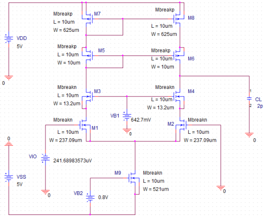
3. Design, Simulation, and Analysis
The single stage Telescopic CMOS operational amplifier has been designed using the proposed schematic layout given in
Figure 7 and the aspect ratios calculated. We have used a double supply voltage of
. The inverting and non-inverting terminals of the circuit were connected to ground. The width and length of the transistors were initially set according to the calculated values in
table 2. But the specifications of current were not meet. Thus, widths of the transistors of device were adjusted through inspection method by repeating the procedure over and over until the desired optimal results were obtained. Redesign was done to meet biasing current and power dissipation specifications by adjusting the widths of the transistors. The modified design with values appearing best for the proposed work is shown in
Figure 8.
3.2. Simulation and Analysis
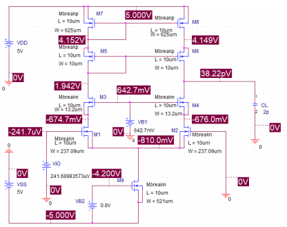
Node Voltage
Ideally, when both inputs of op-amp are grounded (zero volt), the output offset voltage is zero. But practically this is not true. For op-amp designer one main chiriteria is to check the output offset voltage is zero or nearly zero when both inputs are zero. If it is not zero he or she must make the output offset voltage zero or cloth to zero by using input offset voltage. In this design the output offset voltage is not zero, when both inputs were grounded (0V) before using input offset voltage (VIO). But by iterative trial and error method, we were able to reduce the output offset voltage by applying an input offset voltage of 241.68983573µV. The node voltages and the output offset voltage obtained from the PSPICE simulations are shown in the
Figure 9. From the figure we observe that the output offset voltage is an extremely low value which is equal to
(which is almost zero) when both inputs are grounded.
Figure 8. Single-stage Telescopic CMOS op-amp circuit design.
Figure 9. Simulation results of output offset voltage and node voltages.
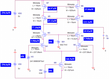
Power Dissipation
Figure 10 shows the simulation results of the power dissipation across each MOS transistor of the single stage Telescopic CMOS op-amp. The total power dissipation (PD) of the circuit is the sum of power dissipation of each transistor. That is:
Thus, the total power consumed by the device is 0.589mW. This shows that the power consumed by the device is too small. Therefore, this device can operate for longer duration of time. The smaller the power dissipation the better the device is. Low power operation is a very important quality factor for batteries that should supply the system for hours or days to power more and more electronic systems.
Figure 10. Simulation result of power dissipation.
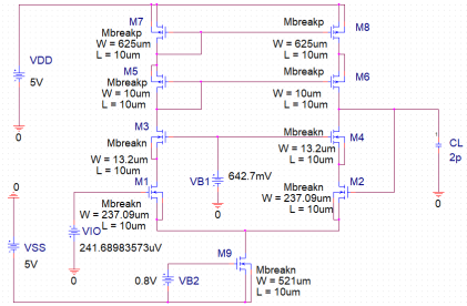
Input Common Mode Range (ICMR)
The circuit design of input common mode range is shown in the
figure 11. For linearity test, the single stage Telescopic CMOS op amp is biased in the unity gain (voltage follower) configuration.
Figure 11. Circuit design to measure ICMR.
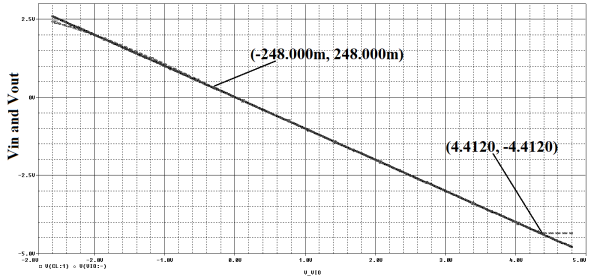
The simulation result of ICMR is shown in the
figure 12. From the figure we can observe that the output voltage of the op-amp is linear for input voltages ranging from -248mV to 4.4120V, for which the output match’s with input in magnitude, but it is inverted due to the input offset voltage applied in the non-inverting terminal is negative. Thus, in this voltage range this op-amp is used as a buffer.
Figure 12. Simulation result of ICMR.
Open Loop Gain, Unity Gain Frequency and Phase Margin:
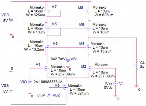
The open loop gain, unity gain frequency (UGB) and phase margin (PM) are measured using the design shown in
figure 13. In this configuration the amplifier is an open loop with ±5V supply voltages. An AC signal of 1V is applied at the inverting input terminal and an input offset voltage of 241.68983573µV is applied to the non-inverting input terminal.
Figure 13. Circuit design to measure the open loop gain, unity gain frequency, cut off frequency, phase difference and phase margin.
The simulation results of the open loop gain and the phase margin are shown in
figure 14. From the figure one can see that the open loop gain is found to be 77.777dB. Besides the cut-off frequency (the 3dB open loop gain frequency) and the unity gain frequency are 1.9598KHz and 7.3053MHz respectively. In addition, we got a phase difference of 179.971 º and phase margin of 80.669º.
Figure 14. Simulation result of open loop gain and PM.
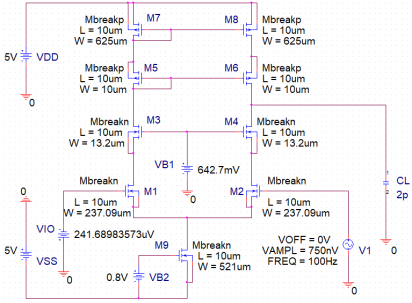
Input and Output Voltage swings:
The circuit design to measure the input and output voltage swings is shown in the
figure 15. The inverting terminal is connected to a sinusoidal voltage source of 750nV amplitude with frequency of 100Hz.
Figure 15. The circuit design to measure input and output voltage swings.
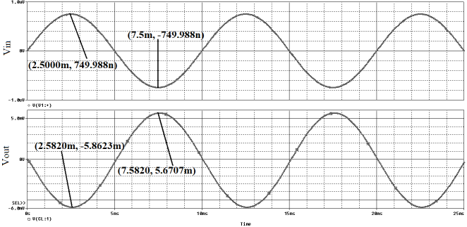
The input and output voltage swing simulation results are displayed in the
figure 16. As we can see from the figure that output AC voltage is amplified but the input AC voltage lags it by π/2; it is because the input is supplied into the inverting terminal of the op-amp. Also, the peak to peak output signal is 11.533mV, when the input peak to peak signal is 1.499976uV.
Figure 16. Simulation result of the input and output voltage swings.
The gain can be calculated by using gain equation as follows:
Where: and are the peak to peak output voltage and the peak to peak input voltages respectively.
Using the values in the gain equation, we get:
In dB scale the gain can be:
Therefore, the output voltage is times the input voltage. The calculated gain is the same as that we have obtained from the graph.
Abbreviations
op-amp: Operational Amplifier
PD: Power Dissipation
AC: Alternating Current
PMOS: Positive Channel MOS
CMOS: Complementary Metal Oxide Semiconductor
SR: Slew Rate
CMRR: Common Mode Rejection Ratio
: Bias Voltage
DC: Direct Current
UGB: Unity Gain Frequency
dB: Decibel
: Drain Voltage
IC: Integrated Circuit
: Voltage from Drain to Source
ICMR: Input Common Mode Range
: Drain to Source Saturation Voltage
Load Capacitance
: Voltage from Gate to Source
Open-Loop Voltage Gain
: Input Voltage
NMOS: Negative Channel MOS
: Output Voltage
: Source Voltage
VIO Input Offset Voltage
: Thresh Hold Voltage for PMOS
: Constant Parameter for NMOS
: Thresh Hold voltage for NMOS
: Constant parameter for PMOS
L: Length
W: Width
: Aspect Ratio
PM: Phase Margin
Acknowledgments
First of all, thanks to GOD and his mother St’Marry for giving me this opportunity and the strength in my success. God is with me everywhere.
Next, I would like to give a special thanks to my advisor Dr Haileeyesus Workineh, at the Bahir Dar University, College of Science, department of Physics, for his excellent guidance, kind support, precious discussion, constant encouragement, useful suggestions and advice, and valuable comments throughout the preparation of this thesis. The completion of this work would have not been possible without his guidance, continuous comments and corrections. Working with him has allowed me to acquire great number of skills as an electronics student, particularly about PSPICE design and simulation software. I greatly respect and admire him. Words are inadequate in offering my thanks to him. I simply say him thank you for everything.
Finally, I would like to express my thanks to all my family members for their love and support.