Because of its excellent flexibility, security, reliability and convenience, wireless power transfer(WPT) has become a research hotspot at home and abroad. Currently available WPT technology has the broadest application prospects and can be used in consumer electronics, household appliances, medical equipment, electric vehicles and many other fields. In low-power wireless charging systems such as electric bicycles, volume and cost of the receiving side are required to be minimized. However, in traditional receiving side circuit, compensation network, sampling circuit and wireless communication circuit make it difficult to reduce the device size and limit further reduction of cost. Aiming at the above problems, a single-switch LC inverter S-S wireless charging circuit with adaptive constant current (CC) and constant voltage (CV) control by transmitting side sensing load changes of receiving side is proposed. In this paper, load-independent CC and CV characteristics and relationship between auxiliary coil voltage and load voltage are derived. The simplest equivalent model of the proposed circuit is developed, the expression for equivalent input voltage is derived, and the constraints of zero-voltage switching (ZVS) are analyzed. Based on the constraint, an iterative method of variable duty cycle is proposed, which can accurately find the duty cycle range in which the ZVS can be realized as well as the peak resonant current in this range, which provides a reference for parametric design of single-switching circuit. Finally, a 5A/54.6V experimental prototype is built to verify the correctness of the proposed theory.
| Published in | American Journal of Electrical Power and Energy Systems (Volume 13, Issue 4) |
| DOI | 10.11648/j.epes.20241304.12 |
| Page(s) | 69-82 |
| Creative Commons |
This is an Open Access article, distributed under the terms of the Creative Commons Attribution 4.0 International License (http://creativecommons.org/licenses/by/4.0/), which permits unrestricted use, distribution and reproduction in any medium or format, provided the original work is properly cited. |
| Copyright |
Copyright © The Author(s), 2024. Published by Science Publishing Group |
Wireless Power Transfer, Constant Current and Constant Voltage, S-S Compensation Topology, Transmitting Side Auxiliary Coil
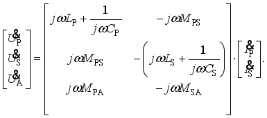
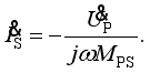
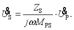
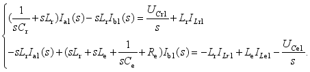
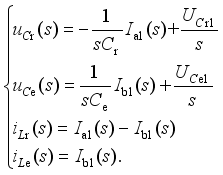
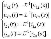
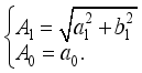
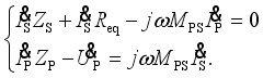
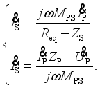
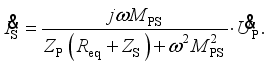
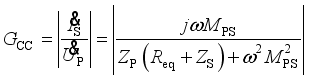
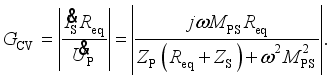
 is the voltage across the capacitor Cr,
  is the input voltage of the rectifier on the receiving side, and
  is the induced voltage across the auxiliary coil LA. According to Kirchhoff’s voltage and current laws, (1) can be obtained
 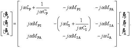 (1)
(1)  (2)
(2)  (3)
(3)  (4)
(4)  (5)
(5)  (6)
(6)  (7)
(7)  (8)
(8)  (9)
(9)  (10)
(10)  (11)
(11)  (12)
(12)  (13)
(13)  (14)
(14) 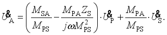 (15)
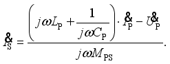
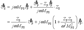
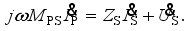
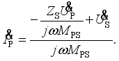
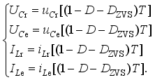
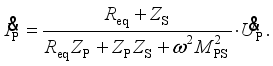
(15)  and the load voltage UB is
  (16)
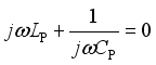
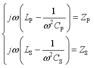
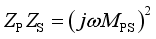
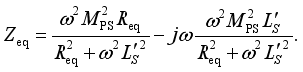
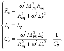
(16)  is only related to the load voltage UB when the mutual inductance is constant. In the electric bicycle charging occasion, the precise alignment between the transmitting coil and the receiving coil can be achieved by means of auxiliary positioning. Therefore, it can be considered that the mutual inductance does not change in actual charging situations.
  (17)
(17)  (18)
(18)  (19)
(19)  (20)
(20)  (21)
(21)  (22)
(22)  (23)
(23)  (24)
(24) 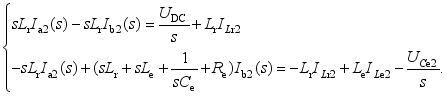 (25)
(25) 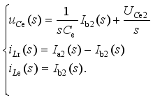 (26)
(26)  (27)
(27)  (28)
(28)  (29)
(29)  (30)
(30)  (31)
(31)  (32)
(32)  (33)
(33)  (34)
(34)  (35)
(35)  (36)
(36)  (37)
(37)  (38)
(38) Symbol | Definition | Value |
|---|---|---|
UDC | Input DC voltage | 48V |
f | Operating frequency | 85kHz |
IB | Output current in constant-current mode | 5.0A |
VB | Output voltage in constant-voltage mode | 54.6V |
PB | Output power | 250W |
 (39)
(39) Symbol | Definition | Value |
|---|---|---|
Cr | Resonant capacitance at the transmitting-side | 117.04nF |
CP1 | Resonant capacitance at the transmitting-side | 58.44nF |
CP2 | Resonant capacitance at the transmitting-side | 44.92nF |
CS | Resonant capacitance at the receiving-side | 116.51nF |
CA | Auxiliary circuit voltage stabilizing capacitor | 19.96 nF |
Lr | Resonant inductance at the transmitting-side | 9.95μH |
LP | Inductance of the transmitter coil | 60.42μH |
LS | Inductance of the receiving coil | 45.13μH |
LA | Inductance of the auxiliary coil | 5.382μH |
NLP | Turns of LP | 23 |
NLS | Turns of LS | 18 |
NLA | Turns of L A | 8 |
MPS | Mutual inductance between LP and LS | 19.70μH |
MPA | Mutual inductance between LP and LA | 4.2375μH |
MSA | Mutual inductance between LS and LA | 1.595μH |
DZVS | Proportion of ZVS | 0.085 |
D | Duty cycle | 0.54 |
h | Transmission distance | 30mm |
Reference | Input DC Voltage | Frequency | Output Power | Number of MOSFETs | Number of secondary resonant devices | Wireless Communication | CC/CV |
|---|---|---|---|---|---|---|---|
Proposed | 48V | 85kHz | 250W | 1 | 1 | No | CC and CV |
[31] | 48V | 100kHz | 130W | 4 | 1 | No | CC and CV |
[32] | 48V | 200kHz | 120W | 4 | 2 | No | CC and CV |
[33] | 120V | 85kHz | 1000W | 4 | 4 | No | CC and CV |
[35] | 200V | 85kHz | 1050W | 6 | 1 | No | CC and CV |
[34] | 155V | 50kHz | 1000W | 6 | 1 | No | CC and CV |
[19] | 64V | 85kHz | 202W | 4 | 1 | No | CC and CV |
[26] | 200V | 85kHz | 1000W | 4 | 4 | / | CC and CV |
[22] | 24V | 100kHz/67kHz | 24W | 1 | 4 | Yes | CC and CV |
[21] | 96V | 100kHz/86.5kHz | 216W | 1 | 3 | Yes | CC and CV |
WPT | Wireless Power Transfer Constant Current |
CC | Constant Current |
CV | Constant Voltage |
ZVS | Zero-Voltage Switching |
| [1] | Y. Shao, H. Zhang, M. Liu, and C. Ma, "Explicit Design of Impedance Matching Networks for Robust MHz WPT Systems With Different Features," IEEE Trans. Power Electron. vol. 37, no. 9, pp. 11382-11393, 2022. |
| [2] | Z. Wei, B. Zhang, S. Lin, and C. Wang, "A Self-oscillation WPT System with High Misalignment Tolerance," IEEE Trans. Power Electron., early access, |
| [3] | H. Yang et al., "A Hybrid Load Matching Method for WPT Systems to Maintain High Efficiency Over Wide Load Range," IEEE Trans. Transp. Electrification. vol. 9, no. 1, pp. 1993-2005, 2023. |
| [4] | Q. Deng et al., "Wired/Wireless Hybrid Charging System for Electrical Vehicles With Minimum Rated Power Requirement for DC Module," IEEE Trans. Veh. Technol. vol. 69, no. 10, pp. 10889-10898, 2020. |
| [5] | A. Hossain, P. Darvish, S. Mekhilef, K. S. Tey, and C. W. Tong, "A New Coil Structure of Dual Transmitters and Dual Receivers With Integrated Decoupling Coils for Increasing Power Transfer and Misalignment Tolerance of Wireless EV Charging System," IEEE Trans. Ind. Electron. vol. 69, no. 8, pp. 7869-7878, 2022. |
| [6] | S. Zhao, C. Xia, Z. Yang, H. Lu, H. Zhang, and C. Lu, "Bipolar Checkerboard Metal Object Detection Without Blind Zone Caused by Excitation Magnetic Field for Stationary EV Wireless Charging System," IEEE Trans. Power Electron. vol. 38, no. 5, pp. 6696-6709, 2023. |
| [7] | I. U. Castillo-Zamora, P. S. Huynh, D. Vincent, F. J. Perez-Pinal, M. A. Rodriguez-Licea, and S. S. Williamson, "Hexagonal Geometry Coil for a WPT High-Power Fast Charging Application," IEEE Trans. Transp. Electrification. vol. 5, no. 4, pp. 946-956, 2019. |
| [8] | Y. Wu, C. Liu, M. Zhou, X. Mao, and Y. Zhang, "An Antioffset Electric Vehicle Wireless Charging System Based on Dual Coupled Antiparallel Coils," IEEE Trans. Power Electron. vol. 38, no. 5, pp. 5634-5637, 2023. |
| [9] | K. Song et al., "A Rotation-Lightweight Wireless Power Transfer System for Solar Wing Driving," IEEE Trans. Power Electron. vol. 34, no. 9, pp. 8816-8830, Sep 2019. |
| [10] | S. Jeong et al., "Smartwatch Strap Wireless Power Transfer System With Flexible PCB Coil and Shielding Material," IEEE Trans. Ind. Electron. vol. 66, no. 5, pp. 4054-4064, May 2019. |
| [11] | S. Pan, Y. Xu, Y. Lu, W. Liu, Y. Li, and R. Mai, "Design of Compact Magnetic Coupler With Low Leakage EMF for AGV Wireless Power Transfer System," IEEE Trans. Ind. Appl. vol. 58, no. 1, pp. 1044-1052, Jan 2022. |
| [12] | Y. Wang, T. Li, M. Zeng, J. Mai, P. Gu, and D. Xu, "An Underwater Simultaneous Wireless Power and Data Transfer System for AUV With High-Rate Full-Duplex Communication," IEEE Trans. Power Electron. vol. 38, no. 1, pp. 619-633, 2023. |
| [13] | Y. Chen et al., "A Clamp Circuit-Based Inductive Power Transfer System With Reconfigurable Rectifier Tolerating Extensive Coupling Variations," IEEE Trans. Power Electron., |
| [14] | H. Shen, P. Tan, B. Song, X. Gao, and B. Zhang, "Receiver Position Estimation Method for Multitransmitter WPT System Based on Machine Learning," IEEE Trans. Ind. Appl. vol. 58, no. 1, pp. 1231-1241, 2022. |
| [15] | W. Zhong, H. Li, S. Y. R. Hui, and M. D. Xu, "Current Overshoot Suppression of Wireless Power Transfer Systems With on–off Keying Modulation," IEEE Trans. Power Electron. vol. 36, no. 3, pp. 2676-2684, 2021. |
| [16] | S. Luo, Z. Yao, Z. Zhang, X. Zhang, and H. Ma, "Balanced Dual-Side LCC Compensation in IPT Systems Implementing Unity Power Factor for Wide Load Range and Misalignment Tolerance," IEEE Trans. Ind. Electron. vol. 70, no. 8, pp. 7796-7809, 2023. |
| [17] | S. Samanta, A. K. Rathore, and D. J. Thrimawithana, "Bidirectional Current-Fed Half-Bridge (C) (LC)-(LC) Configuration for Inductive Wireless Power Transfer System," IEEE Trans. Ind. Appl. vol. 53, no. 4, pp. 4053-4062, Jul-Aug 2017. |
| [18] | C. Qi, G. Zheng, Y. Liu, J. Liang, H. Wang, and M. Fu, "A Simplified Three-Order Small-Signal Model for Capacitive Power Transfer System Using Series Compensation," IEEE Trans. Power Electron. vol. 38, no. 5, pp. 5688-5692, 2023. |
| [19] | H. Yuan, C. Wang, and D. Xia, "Research on Input-Parallel Single-Switch WPT System With Load-Independent Constant Voltage Output," IEEE Trans. Transp. Electrification. vol. 9, no. 1, pp. 1888-1896, 2023. |
| [20] | Z. Li, H. Liu, Y. Tian, and Y. Liu, "Constant Current/Voltage Charging for Primary-Side Controlled Wireless Charging System Without Using Dual-Side Communication," IEEE Trans. Power Electron. vol. 36, no. 12, pp. 13562-13577, Dec 2021. |
| [21] | Q. Zhang et al., "Research on Input-Parallel Single-Switch Wireless Power Transfer System With Constant-Current and Constant-Voltage Output," IEEE Trans. Power Electron. vol. 37, no. 4, pp. 4817-4830, Apr 2022. |
| [22] | J. Wang, C. Wang, Z. Lu, Z. Guo, and S. Wang, "Single-Switch Wireless-Power-Transfer Circuit With P-CLC Compensation Network Used for Battery Charging," IEEE Trans. Transp. Electrification. vol. 8, no. 3, pp. 4014-4026, Sep 2022. |
| [23] | R. Yue, C. Wang, H. Li, and Y. Liu, "Constant-Voltage and Constant-Current Output Using P-CLCL Compensation Circuit for Single-Switch Inductive Power Transfer," IEEE Trans. Power Electron. vol. 36, no. 5, pp. 5181-5190, May 2021. |
| [24] | A. Bharadwaj, A. Sharma, and C. C. Reddy, "An Unconventional Measurement Technique to Estimate Power Transfer Efficiency in Series–Series Resonant WPT System Using S-Parameters," IEEE Transactions on Instrumentation and Measurement vol. 71, pp. 1-9, 2022. |
| [25] | Y. Li et al., "A New Coil Structure and Its Optimization Design With Constant Output Voltage and Constant Output Current for Electric Vehicle Dynamic Wireless Charging," IEEE Trans. Ind. Inform. vol. 15, no. 9, pp. 5244-5256, Sep 2019. |
| [26] | H. Li, Y. Yang, J. Chen, J. Xu, M. Liu, and Y. Wang, "A Hybrid Class-E Topology With Constant Current and Constant Voltage Output for Light EVs Wireless Charging Application," IEEE Trans. Transp. Electrification. vol. 7, no. 4, pp. 2168-2180, Dec 2021. |
| [27] | D. Wang, X. Qu, Y. Yao, and P. Yang, "Hybrid Inductive-Power-Transfer Battery Chargers for Electric Vehicle Onboard Charging With Configurable Charging Profile," IEEE Trans. Intell. Transp. Syst. vol. 22, no. 1, pp. 592-599, Jan 2021. |
| [28] | Y. Zhang, Z. Shen, W. Pan, H. Wang, Y. Wu, and X. Mao, "Constant Current and Constant Voltage Charging of Wireless Power Transfer System Based on Three-Coil Structure," IEEE Trans. Ind. Electron. vol. 70, no. 1, pp. 1066-1070, Jan 2023. |
| [29] | J. Cai, X. Wu, P. Sun, Q. Deng, J. Sun, and H. Zhou, "Design of Constant-Voltage and Constant-Current Output Modes of Double-Sided LCC Inductive Power Transfer System for Variable Coupling Conditions," IEEE Trans. Power Electron. vol. 39, no. 1, pp. 1676-1689, Jan 2024. |
| [30] | Z. Luo, Y. Zhao, M. Xiong, X. Wei, and H. Dai, "A Self-Tuning LCC/LCC System Based on Switch-Controlled Capacitors for Constant-Power Wireless Electric Vehicle Charging," IEEE Trans. Ind. Electron. vol. 70, no. 1, pp. 709-720, Jan 2023. |
| [31] | X. Zhu et al., "High-Efficiency WPT System for CC/CV Charging Based on Double-Half-Bridge Inverter Topology With Variable Inductors," IEEE Trans. Power Electron. vol. 37, no. 2, pp. 2437-2448, Feb 2022. |
| [32] | Z. Huang, G. Wang, J. Yu, and X. Qu, "A Novel Clamp Coil Assisted IPT Battery Charger With Inherent CC-to-CV Transition Capability," IEEE Trans. Power Electron. vol. 36, no. 8, pp. 8607-8611, Aug 2021. |
| [33] | G. Li and H. Ma, "A Hybrid IPT System With High-Misalignment Tolerance and Inherent CC-CV Output Characteristics for EVs Charging Applications," IEEE J. Emerg. Sel. Topics Power Electron. vol. 10, no. 3, pp. 3152-3160, Jun 2022. |
| [34] | C. Ma, R. Yao, C. Li, and X. Qu, "A Family of IPT Battery Chargers With Small Clamp Coil for Configurable and Self-Sustained Battery Charging Profile," IEEE Trans. Power Electron. vol. 38, no. 6, pp. 7910-7919, Jun 2023. |
| [35] | I. W. Iam et al., "Constant-Frequency and Noncommunication-Based Inductive Power Transfer Converter for Battery Charging," IEEE J. Emerg. Sel. Topics Power Electron. vol. 10, no. 2, pp. 2147-2162, Apr 2022. |
| [36] | V. Yenil and S. Cetin, "Load Independent Constant Current and Constant Voltage Control of LCC-Series Compensated Wireless EV Charger," IEEE Trans. Power Electron. vol. 37, no. 7, pp. 8701-8712, Jul 2022. |
| [37] | Z. Guo, C. Wang, S. Lin, L. Yang, and X. Lu, "Multiparallel and Flexible Expansion of Single-Switch WPT Inverter by Magnetic Integration," IEEE Trans. Power Electron. vol. 38, no. 3, pp. 4167-4180, Mar 2023. |
| [38] | G. Ke, Q. Chen, S. Zhang, X. Xu, and L. Xu, "A Single-Ended Hybrid Resonant Converter With High Misalignment Tolerance," IEEE Trans. Power Electron. vol. 37, no. 10, pp. 12841-12852, Oct 2022. |
APA Style
Lin, S., Zheng, J., Lu, Y., Zhao, F., Wang, C. (2024). Single-Switch Inverter Wireless Charger with Adaptive Constant Current and Constant Voltage Control by Transmitting Side Sensing Load Changes of Receiving Side. American Journal of Electrical Power and Energy Systems, 13(4), 69-82. https://doi.org/10.11648/j.epes.20241304.12
ACS Style
Lin, S.; Zheng, J.; Lu, Y.; Zhao, F.; Wang, C. Single-Switch Inverter Wireless Charger with Adaptive Constant Current and Constant Voltage Control by Transmitting Side Sensing Load Changes of Receiving Side. Am. J. Electr. Power Energy Syst. 2024, 13(4), 69-82. doi: 10.11648/j.epes.20241304.12
AMA Style
Lin S, Zheng J, Lu Y, Zhao F, Wang C. Single-Switch Inverter Wireless Charger with Adaptive Constant Current and Constant Voltage Control by Transmitting Side Sensing Load Changes of Receiving Side. Am J Electr Power Energy Syst. 2024;13(4):69-82. doi: 10.11648/j.epes.20241304.12
@article{10.11648/j.epes.20241304.12,
  author = {Shan Lin and Jianfen Zheng and Yun Lu and Fei Zhao and Chunfang Wang},
  title = {Single-Switch Inverter Wireless Charger with Adaptive Constant Current and Constant Voltage Control by Transmitting Side Sensing Load Changes of Receiving Side
},
  journal = {American Journal of Electrical Power and Energy Systems},
  volume = {13},
  number = {4},
  pages = {69-82},
  doi = {10.11648/j.epes.20241304.12},
  url = {https://doi.org/10.11648/j.epes.20241304.12},
  eprint = {https://article.sciencepublishinggroup.com/pdf/10.11648.j.epes.20241304.12},
  abstract = {Because of its excellent flexibility, security, reliability and convenience, wireless power transfer(WPT) has become a research hotspot at home and abroad. Currently available WPT technology has the broadest application prospects and can be used in consumer electronics, household appliances, medical equipment, electric vehicles and many other fields. In low-power wireless charging systems such as electric bicycles, volume and cost of the receiving side are required to be minimized. However, in traditional receiving side circuit, compensation network, sampling circuit and wireless communication circuit make it difficult to reduce the device size and limit further reduction of cost. Aiming at the above problems, a single-switch LC inverter S-S wireless charging circuit with adaptive constant current (CC) and constant voltage (CV) control by transmitting side sensing load changes of receiving side is proposed. In this paper, load-independent CC and CV characteristics and relationship between auxiliary coil voltage and load voltage are derived. The simplest equivalent model of the proposed circuit is developed, the expression for equivalent input voltage is derived, and the constraints of zero-voltage switching (ZVS) are analyzed. Based on the constraint, an iterative method of variable duty cycle is proposed, which can accurately find the duty cycle range in which the ZVS can be realized as well as the peak resonant current in this range, which provides a reference for parametric design of single-switching circuit. Finally, a 5A/54.6V experimental prototype is built to verify the correctness of the proposed theory.
},
 year = {2024}
}
TY  - JOUR
T1  - Single-Switch Inverter Wireless Charger with Adaptive Constant Current and Constant Voltage Control by Transmitting Side Sensing Load Changes of Receiving Side

AU  - Shan Lin
AU  - Jianfen Zheng
AU  - Yun Lu
AU  - Fei Zhao
AU  - Chunfang Wang
Y1  - 2024/12/25
PY  - 2024
N1  - https://doi.org/10.11648/j.epes.20241304.12
DO  - 10.11648/j.epes.20241304.12
T2  - American Journal of Electrical Power and Energy Systems
JF  - American Journal of Electrical Power and Energy Systems
JO  - American Journal of Electrical Power and Energy Systems
SP  - 69
EP  - 82
PB  - Science Publishing Group
SN  - 2326-9200
UR  - https://doi.org/10.11648/j.epes.20241304.12
AB  - Because of its excellent flexibility, security, reliability and convenience, wireless power transfer(WPT) has become a research hotspot at home and abroad. Currently available WPT technology has the broadest application prospects and can be used in consumer electronics, household appliances, medical equipment, electric vehicles and many other fields. In low-power wireless charging systems such as electric bicycles, volume and cost of the receiving side are required to be minimized. However, in traditional receiving side circuit, compensation network, sampling circuit and wireless communication circuit make it difficult to reduce the device size and limit further reduction of cost. Aiming at the above problems, a single-switch LC inverter S-S wireless charging circuit with adaptive constant current (CC) and constant voltage (CV) control by transmitting side sensing load changes of receiving side is proposed. In this paper, load-independent CC and CV characteristics and relationship between auxiliary coil voltage and load voltage are derived. The simplest equivalent model of the proposed circuit is developed, the expression for equivalent input voltage is derived, and the constraints of zero-voltage switching (ZVS) are analyzed. Based on the constraint, an iterative method of variable duty cycle is proposed, which can accurately find the duty cycle range in which the ZVS can be realized as well as the peak resonant current in this range, which provides a reference for parametric design of single-switching circuit. Finally, a 5A/54.6V experimental prototype is built to verify the correctness of the proposed theory.

VL  - 13
IS  - 4
ER  -
Guanzhou Metro Design & Research Institute Co., Ltd., Guanzhou, China
College of Electrical Engineering, Qingdao University, Qingdao, China
Guanzhou Metro Design & Research Institute Co., Ltd., Guanzhou, China
Yunlu New Energy Technology Co., Ltd., Qingdao, China
College of Electrical Engineering, Qingdao University, Qingdao, China
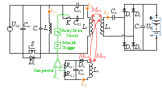
Figure 1. The proposed circuit topology.
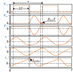
Figure 2. Working waveform of single-switch circuit.
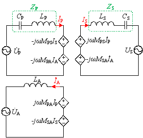
Figure 3. Controlled source equivalent model of the proposed WPT model.
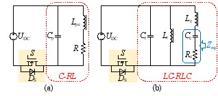
Figure 4. The simplest equivalent circuit of single-switch topology. (a) C-RL form (b) LC-RLC form.
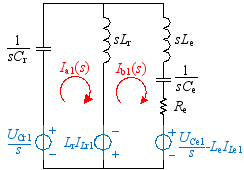
Figure 5. LC-RLC complex frequency domain model in state 1.
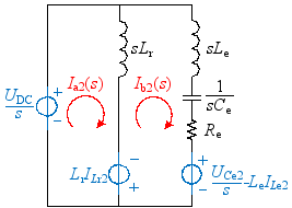
Figure 6. LC-RLC complex frequency domain model in state 2.
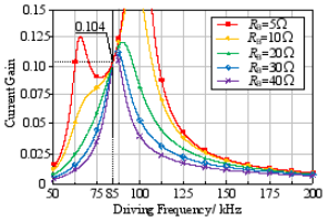
Figure 7. Relationship between current gain and driving frequency.
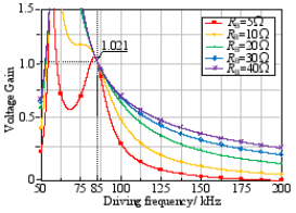
Figure 8. Relationship between voltage gain and driving frequency.
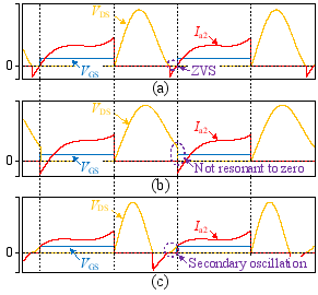
Figure 9. ZVS of single-switch circuit (a) normal condition (b) VDS cannot be reduced to zero (c) VDS secondary oscillation.
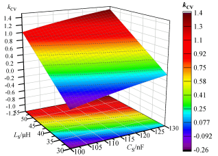
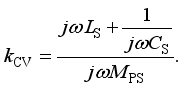
Figure 10. Relationship between kCV and LS and CS.
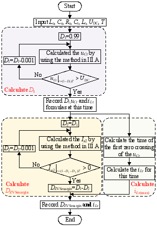
Figure 11. Flow chart of calculating DZVSmargin and iLr(max) with variable duty cycle.
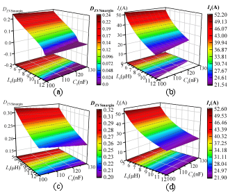
Figure 12. Relationship between DZVSmargin and LS and CS in (a) CC mode (c) CV mode. Relationship between iLr(max) and LS and CS in (b) CC mode (d) CV mode.
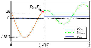
Figure 13. Mathematica simulates VCr waveform.
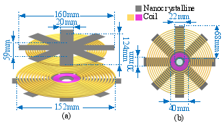
Figure 14. Magnetic coupler model. (a) Overall view of magnetic coupler (b) top view of transmitting side.
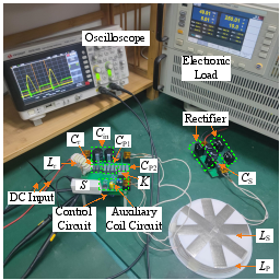
Figure 15. Photo of the proposed circuit.
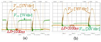
Figure 16. Switching ZVS and voltage stress waveforms in (a) CC mode, (b) CV mode.
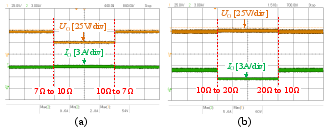
Figure 17. Variable load experiment (a) CC mode (b) CV mode.
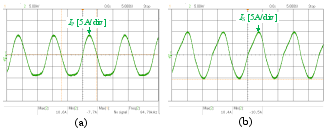
Figure 18. At rated load RB=10Ω (a) transmitting coil current IP (b) receiving coil current IS.
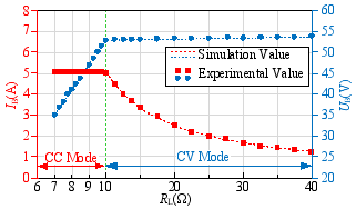
Figure 19. System CC and CV output.
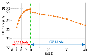
Figure 20. System efficiency.
Information