Abstract
Silicon ingots can be crystallized using a variety of processes. These lead to different qualities of crystal, and therefore of solar cell, depending on whether the silicon obtained is polycrystalline, i.e. made up of a multitude of crystals of varying size and orientation, or monocrystalline, i.e. formed from a single crystal. Like crystallization, doping is one of the steps in the silicon manufacturing process. Studying the doping level of a solar cell is crucial, as it has a direct influence on its performance, particularly its ability to convert sunlight into electricity. Doping, which consists in introducing impurities into silicon, modifies the electrical properties of the material and, consequently, the characteristics of the solar cell. The aim of this study is to assess the impact of polycrystalline crystal size and the capture effect at the contact surface of two crystals on the effect of p-layer dopant on effective diffusion length, diode current, short-circuit current and open-circuit voltage. Using the continuity equation with generation-recombination phenomena, this study found mathematical expressions for the fundamental electrical parameters needed to characterize solar cells. These mathematical expressions relate the effective diffusion length, diode current and electrical parameters such as short-circuit current and open-circuit voltage to the p-layer doping rate, crystal dimensions and carrier loss rate at the interfaces, respectively. Then, using Mathcad software, we simulated the impact of crystal size and the effect of captures at crystal interfaces on the influence of p-layer doping rate on effective diffusion length, diode current and electrical parameters such as Jsc and Voc. The results obtained from this analysis reveal that: For low values of p-layer doping rate and crystal size, the short-circuit current and effective diffusion length decrease less with low p-layer doping rates. On the other hand, for p-layer doping rates higher than 1017cm-3, the effective diffusion length and short-circuit current intensity decrease, but this decrease is faster when the crystal size is smaller. Diode current and open-circuit voltage increase with p-layer doping rate and crystal size. Growth is greatest when the p-layer doping rate is greater than 1017 cm-3 for diode current. The results of this study make it possible to design more efficient solar cells for polycrystalline silicon photovoltaic applications by keeping the doping rate at or below 1017 cm-3.
Keywords
Short-circuit Current, Diode Current, Effective Diffusion Length, Open-circuit Voltage
1. Introduction
Polycrystalline silicon is made up of assembled crystals ranging in size from 1mm to around 2 cm, known as “grains”. This material, which is less efficient than monocrystalline silicon, is produced in large foundry crucibles, by melting and cooling blocks of purified silicon. This is the most widely used silicon today, with yields ranging from 12% to 15%.
The standard manufacturing process for photovoltaic systems involves several stages. These include doping, which consists in modifying the conductivity of silicon by injecting impurity atoms.
The silicon is purified, then uniformly doped and cut into wafers once cooled. The crystallization technique consists of gradually solidifying the molten polycrystalline silicon in a controlled manner. The doping element, usually boron, is added to the molten silicon charge to give p-type doping
| [1] | Yong Zhao; Chunjun Liang; Mengjie Sun; Qian Liu; Fujun Zhang; Dan Li; Zhiqun He (2014) Effect of doping on the short-circuit current and open-circuit voltage of polymer solar cells. Appl. Phys. 116, 154506: http://dx.doi.org/10.1063/1.4898692 |
| [2] | Traore, S., Diedhiou, A., Sambou, A. and Camara, M. (2024) Study of the Electrical Parameters of a Silicon Solar Cell (n+/p/p+) under the Effect of Tempera ture by Optimization of the Base Thickness and the Doping Rate. Journal of Materials Science and Chemical Engineering, 12, 15-23. https://doi.org/10.4236/msce.2024.1211002 |
| [3] | Thiame, M., Camara, M., Lemrabott, H., Lemine Cheikh, M., Gueye, S. and Sissoko, G. (2023) Étude a 3d de la photopile au silicium polycristallin: Optimisation du taux de dopage en fonction de l’épaisseur de la base. International Journal of Advanced Research, 11, 311-322. https://doi.org/10.21474/ijar01/17989 |
| [4] | Sada Traore, Ansoumane Diedhiou and Momath Ndiaye (2024) Study of the performance parameters of a silicon solar cell (n+/p/p+) in frequency modulation placed in a medium dominated by the magnetic field: Effect of low and high doping rate Journal of Engineering and Technology Research Vol. 16(2), pp. 23-28 http://www.academicjournals.org/JETR |
[1-4]
. Many studies have focused on the doping of photovoltaic cells
| [1] | Yong Zhao; Chunjun Liang; Mengjie Sun; Qian Liu; Fujun Zhang; Dan Li; Zhiqun He (2014) Effect of doping on the short-circuit current and open-circuit voltage of polymer solar cells. Appl. Phys. 116, 154506: http://dx.doi.org/10.1063/1.4898692 |
| [2] | Traore, S., Diedhiou, A., Sambou, A. and Camara, M. (2024) Study of the Electrical Parameters of a Silicon Solar Cell (n+/p/p+) under the Effect of Tempera ture by Optimization of the Base Thickness and the Doping Rate. Journal of Materials Science and Chemical Engineering, 12, 15-23. https://doi.org/10.4236/msce.2024.1211002 |
| [3] | Thiame, M., Camara, M., Lemrabott, H., Lemine Cheikh, M., Gueye, S. and Sissoko, G. (2023) Étude a 3d de la photopile au silicium polycristallin: Optimisation du taux de dopage en fonction de l’épaisseur de la base. International Journal of Advanced Research, 11, 311-322. https://doi.org/10.21474/ijar01/17989 |
| [4] | Sada Traore, Ansoumane Diedhiou and Momath Ndiaye (2024) Study of the performance parameters of a silicon solar cell (n+/p/p+) in frequency modulation placed in a medium dominated by the magnetic field: Effect of low and high doping rate Journal of Engineering and Technology Research Vol. 16(2), pp. 23-28 http://www.academicjournals.org/JETR |
| [5] | Camara, M., Ba, M. L., Diop, G., Ba, A. M., Diatta, I., Thiame, M., and Sissoko, G. (2020). 3D modelling study of silicon solar cell: effet of doping rate and grain Size, Journal of Scientific and Engineering, Research, 7(10), 14-24. |
| [6] | Ramatou Konate, Bernard Zouma, a), Mahamadi Savadogo, Fabe Idrissa Barro, Issa Zerbo, Martial Zoungrana, and Dieudonné Joseph Bathiebo (2023) Impacts of the Base and Emitter Doping Rate on the Internal Quantum Efficiency https://doi.org/10.1063/5.0177051 |
| [7] | F. I. Barro et al. (2015) “Theoretical investigation of base doping and illumination level effects on a bifacial silicon solar cell,” Br. J. Appl. Sci. Technol. 7(6), 610–618 (2015). https://doi.org/10.9734/BJAST/2015/15628 |
[1-7]
, as this is an important stage in the manufacture of solar cells. Recent studies have modelled the effect of doping rate on electrical parameters
| [2] | Traore, S., Diedhiou, A., Sambou, A. and Camara, M. (2024) Study of the Electrical Parameters of a Silicon Solar Cell (n+/p/p+) under the Effect of Tempera ture by Optimization of the Base Thickness and the Doping Rate. Journal of Materials Science and Chemical Engineering, 12, 15-23. https://doi.org/10.4236/msce.2024.1211002 |
| [4] | Sada Traore, Ansoumane Diedhiou and Momath Ndiaye (2024) Study of the performance parameters of a silicon solar cell (n+/p/p+) in frequency modulation placed in a medium dominated by the magnetic field: Effect of low and high doping rate Journal of Engineering and Technology Research Vol. 16(2), pp. 23-28 http://www.academicjournals.org/JETR |
[2, 4]
. We now take into account the effective diffusion length and diode current. However, the diode current, which models losses in the transition zone, and the effective diffusion length are highly dependent on the doping rate and crystal dimensions.
Thus, in this manuscript, we will evaluate the impact of crystal dimensions and capture effects at their interfaces on the effect of p-layer dopant content on effective diffusion length, diode current, short-circuit current (Jcc) and open-circuit voltage (Vco).
We began with a theoretical study that enabled us to establish analytical expressions for our various quantities as a function of crystal dimensions, the capture effect at interfaces and impurity content. Then, using Mathcad software, we simulated the impact of these parameters on effective diffusion length, diode current, short-circuit current and open-circuit voltage.
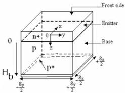
2. Three Dimensional Modeling of the Monofacial Polycrystalline Silicon Solar Cell
The three-dimensional model used is that of a polycrystalline silicon crystal whose dimensions are limited as follows: from 0 to Hb along the z axis whose origin is taken from the junction and is none other than the center of the crystal, from -gx/2 to 0 and 0 to +gx/2 along the x axis and finally from -gy/2 to 0 and 0 to +gy/2 along the y axis. The mathematical equations given in the paragraph below are obtained taking into account certain assumptions such as
| [8] | Diallo, H. L., Seïdou Maiga, A., Wereme, A. and Sissoko, G. (2008) New Approach of Both Junction and Back Surface Recombination Velocities in a 3D Modelling Study of a Polycrystalline Silicon Solar Cell. The European Physical Journal Applied Phys ics, 42, 203-211. https://doi.org/10.1051/epjap:2008085 |
| [9] | Omar M., Thiame M., LY I., Datta I., Diouf M. S., Traore Y., Ndiaye M. and Sissoko G., (2016). 3D Study of a Polycrystalline Bifacial Silicon Solar Cell, Illuminated Simultaneously by Both Sides: Grain Size and Recombination Velocity Influence. International Journal of Innovative Science, Engineering & Technology, Vol. 3 Issue 12, pp. 152-162 http://www.ijiset.com |
| [10] | M. Thiame, A. Diene, B. Seibou, Cheick. Tidiane. Sarr, M. L. O. Cheikh, Ibrahima. Diatta, M. Dieye, Youssou. Traoré, Gregoire. Sissoko, (2017). 3D Study of a Bifacial Polycrystalline Silicon Solar Cell Back Surface Illuminated: Influence of Grain Size and Recombination Velocity, JSER. 4(1) pp 135-145. |
[8-10]
:
Crystal dimensions along x and y are the same.
An anti-reflective layer on the n+ layer, which receives polychromatic radiation.
Carrier concentration along x and y is identical; generation rate is a function of z.
Recombination planes are perpendicular to the O x and O y axes.
The contribution of the n+ layer is negligible compared to that of the p layer.
Only the electric field at the transition zone is taken into account.
Crystal interfaces are perpendicular to the transition zone.
Figure 1. Geometry of the crystal model used.
3. Continuity Equation with Generation-recombination Phenomena
Since our analysis is limited to the p-layer, we present the three-dimensional continuity equations for p-layer carriers in the static regime under polychromatic illumination.
| [8] | Diallo, H. L., Seïdou Maiga, A., Wereme, A. and Sissoko, G. (2008) New Approach of Both Junction and Back Surface Recombination Velocities in a 3D Modelling Study of a Polycrystalline Silicon Solar Cell. The European Physical Journal Applied Phys ics, 42, 203-211. https://doi.org/10.1051/epjap:2008085 |
| [11] | Mountaga Boiro, Amadou Diao, Adama Ndiaye, Diène Gackou (2024) Influence of Wavelength on the Diffusion Capacitance of a Serial Vertical Junction Silicon Solar Cell in Frequency Regime American Journal of Materials Science and Engineering, 2024, Vol. 12, No. 2, 25-29 Available online at http://pubs.sciepub.com/ajmse/12/2/1 |
| [12] | Moussa Camara, Mamoudou Toure, Haba Siba, Mahamat Batran Mouta, Ousmane Fanta Camara and Moustapha Thiame (2025) Analyse of Impact of Temperature, Grain Size, and Magnetic Field on Effective Diffusion, Asian Journal of Science and Technology 16, (02), 13516-13519 at http://www.journalajst.com |
| [13] | Moussa Camara, Moustapha Thiame, Mamoudou Touré, Haba Siba and Ousmane Fanta Camara 1 (2025) Effect of Crystal Size on the Optimum Temperature for the Highest Capacity of Tree-Dimensional Polycrystalline Silicon Solar Cell, Int. J. Adv. Res. 13(01), 443-452 https://dx.doi.org/10.21474/IJAR01/20215 |
| [14] | Mayoro D., Senghane Mb, Martial Z., Issa Z., Biram D., Gregoire S. (2015) A 3D Modelling of Solar Cell’s Electric Power under Real Operating Point World Journal of Condensed Matter Physics, 2015, 5, 275-283 http://dx.doi.org/10.4236/wjcmp.2015.54028 |
| [15] | Kosso AM. M., Thiame M., Youssou. T., Ibrahima D., Malick Nd., Lemrabott H., Ibrahima L., Gregoire. Sissoko, (2018). 3D Study of a Silicon Solar Cell under Constant Monochromatic Illumination: Influence of Both, Temperature and Magnetic Field. Journal of Scientific and Engineering Research, 5(7), pp. 259-269 online http://www.jsaer.com |
| [16] | Ramatou K., Bernard Z., Adama O., Bruno K., Martial Z., Sié K (2022) Impact of the Thicknesses of the p and p+ Regions on the Electrical Parameters of a Bifacial PV Cell Energy and Power Engineering, 2022, 14, 133-145 https://www.scirp.org/journal/epe |
| [17] | Fabe. I. B et al. “On the capacitance of crystalline silicon solar cells in steady state,” Turk. J. Phys. 39, 122–127 (2015). https://doi.org/10.3906/fiz-1408-3 |
[8, 11-17]
.
(1)
𝛅n(x, y, z) is the electron density in the p-layer.
Ln and Dn are the length and transition coefficient, respectively, of the p-layer electrons across the n+/p transition region.
Nb is the dopant level of layer p.
The solar cell is illuminated from the side covered by an anti-reflective coating, so the expression of the generation rate G
n(z) is
| [6] | Ramatou Konate, Bernard Zouma, a), Mahamadi Savadogo, Fabe Idrissa Barro, Issa Zerbo, Martial Zoungrana, and Dieudonné Joseph Bathiebo (2023) Impacts of the Base and Emitter Doping Rate on the Internal Quantum Efficiency https://doi.org/10.1063/5.0177051 |
| [8] | Diallo, H. L., Seïdou Maiga, A., Wereme, A. and Sissoko, G. (2008) New Approach of Both Junction and Back Surface Recombination Velocities in a 3D Modelling Study of a Polycrystalline Silicon Solar Cell. The European Physical Journal Applied Phys ics, 42, 203-211. https://doi.org/10.1051/epjap:2008085 |
| [9] | Omar M., Thiame M., LY I., Datta I., Diouf M. S., Traore Y., Ndiaye M. and Sissoko G., (2016). 3D Study of a Polycrystalline Bifacial Silicon Solar Cell, Illuminated Simultaneously by Both Sides: Grain Size and Recombination Velocity Influence. International Journal of Innovative Science, Engineering & Technology, Vol. 3 Issue 12, pp. 152-162 http://www.ijiset.com |
| [10] | M. Thiame, A. Diene, B. Seibou, Cheick. Tidiane. Sarr, M. L. O. Cheikh, Ibrahima. Diatta, M. Dieye, Youssou. Traoré, Gregoire. Sissoko, (2017). 3D Study of a Bifacial Polycrystalline Silicon Solar Cell Back Surface Illuminated: Influence of Grain Size and Recombination Velocity, JSER. 4(1) pp 135-145. |
[6, 8-10]
:
(2)
ai, and bi coefficients deduced from solar luminosity.
z is the depth of light penetration in the p layer.
The expression for the carrier density given by equation
(
3) is the solution to equation
(
1)
| [2] | Traore, S., Diedhiou, A., Sambou, A. and Camara, M. (2024) Study of the Electrical Parameters of a Silicon Solar Cell (n+/p/p+) under the Effect of Tempera ture by Optimization of the Base Thickness and the Doping Rate. Journal of Materials Science and Chemical Engineering, 12, 15-23. https://doi.org/10.4236/msce.2024.1211002 |
[2]
.
(3)
We obtained equation
(
4) by replacing the carrier density in equation
(
3) with its expression given by equation
(
6). With equation
(
8), the solution to equation
(
7) is.
(4)
Ln
kx,jy and Z
kx,jy are respectively the effective diffusion length and the solution of equation
(
4).
(5)
et given by the boundary conditions at the surfaces bounding the p layer along the z axis:
At layer n+ or z=0
(6)
At the p+ layer or z=H
(7)
are obtained through crystal boundary conditions along the x and y axes, they model the effect of carrier capture at crystal interfaces:
Following x
(8)
Following y
(9)
Scs the rate of loss of carriers at the contact surface between two crystals.
4. Short-circuit Current Density
The short-circuit is identical to the passage of all carriers through the cell's transition zone. The short-circuit current is therefore a parameter used to assess the performance of the solar cell. Its expression is given by equation
(
10)
| [7] | F. I. Barro et al. (2015) “Theoretical investigation of base doping and illumination level effects on a bifacial silicon solar cell,” Br. J. Appl. Sci. Technol. 7(6), 610–618 (2015). https://doi.org/10.9734/BJAST/2015/15628 |
[7]
, which takes into account the contributions of the base, the crystal dimensions and the capture effect at the crystal boundaries.
(10)
q the charge of an electron of layer p.
Sfe is the recombination rate of electrons from the p layer to the n+/p transition zone. It includes two terms: Sfe =Sf0 + Sfj with:
Sf0e the loss at the level of the transition zone when one is in open circuit and Sfj which highlights the electron flow of the p layer having passed through the transition zone.
5. Open-circuit Voltage
Like the short-circuit current, the open-circuit voltage is a quantity that allows us to evaluate the performance of solar cells; it is determined according to given conditions: state of charge, temperature, lighting, etc.
For its evaluation, its expression
| [7] | F. I. Barro et al. (2015) “Theoretical investigation of base doping and illumination level effects on a bifacial silicon solar cell,” Br. J. Appl. Sci. Technol. 7(6), 610–618 (2015). https://doi.org/10.9734/BJAST/2015/15628 |
[7]
, which links it to the dopant levels of the p-layer, the crystal dimensions and the capture effect at the crystal boundaries is:
(11)
ni is the concentration of the crystal before doping.
6. Diode Current
The diode current models the losses in the n+/p transition zone. It exists when the solar cell is exposed.
Its expression
| [7] | F. I. Barro et al. (2015) “Theoretical investigation of base doping and illumination level effects on a bifacial silicon solar cell,” Br. J. Appl. Sci. Technol. 7(6), 610–618 (2015). https://doi.org/10.9734/BJAST/2015/15628 |
[7]
, which links it to the dopant levels of the p-layer, the crystal dimensions and the capture effect at the crystal boundaries is:
(12)
7. Results and Discussion
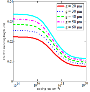
7.1. Influence of the Grain Size on the Effect of the Doping Rate on the Effective Diffusion Length
The effective diffusion length is the effective length traveled by electrons before recombining, which depends on the diffusion length, the dimensions of the crystal, the loss rate at the contact surface between two crystals
| [8] | Diallo, H. L., Seïdou Maiga, A., Wereme, A. and Sissoko, G. (2008) New Approach of Both Junction and Back Surface Recombination Velocities in a 3D Modelling Study of a Polycrystalline Silicon Solar Cell. The European Physical Journal Applied Phys ics, 42, 203-211. https://doi.org/10.1051/epjap:2008085 |
| [18] | J. Oualid, M. Bonfils, J. P. Crest, G. Mathian, H. Amzil, J. Dugas, M. Zehaf and S. Martinuzzi, (1982). «Photocurrent and Diffusion Lengths at the Vicinity of Grain Boundaries (g.b.) in N and P-type Polysilicon. Evaluation of the g.b. Recombination Velocity». Revue Phys. Appl. 17, pp. 119-124. https://doi.org/10.1051/rphysap:01982001703011900 |
[8, 18]
and now of the dopant proportion of layer p.
To evaluate the effect of crystal size on the impact of the p-layer dopant proportion on the effective carrier diffusion length in the p-layer, we presented in
Figure 2 the pattern of the effective diffusion length as a function of the proportion of the dopant for some values of the following dimensions x (gx) and y (gy) of the crystal.
Figure 2. Profile of the effective diffusion length as a function of the p-layer dopant concentration for different crystal dimensions: Sgs = 103 cm/s.
In
figure 2, we notice 3 areas:
A first zone for dopant levels ranging from 1014 cm-3 to 1015 cm-3 where the effective diffusion length remains constant. In this area, the effective diffusion length is almost insensitive to the variation of the dopant level.
A second zone for dopant levels ranging from 3.1015 cm-3 to 1017 cm-3, where the effective diffusion length decreases slightly with the dopant level. Which is explained by a decrease in the lifetime of charge carriers with the concentration of the dopant.
A third area ranging from 1017cm-3 to 1018cm-3 whose diffusion length decreases considerably with the concentration of the dopant to become constant for dopant levels greater than 1018 cm-3. In this area, the material tends to lose these semiconductor properties to become a conductor if we keep doping it.
We also analyze an increase in the effective diffusion length with the dimensions (following x and y) of the crystal as shown by J. Dugas and all in 1987. This increase in the diffusion length can be explained by the fact that the increase in the dimensions of the crystal decreases the density of the recombination centers and the capture effect at the interfaces. We also find that, the effective diffusion length increases strongly with the size of the crystal for low dopant concentrations (for zones 1 and 2). So for low values of p-layer doping rate and crystal size, the effective diffusion length decreases less with low p-layer doping rates. For p-layer doping rates greater than 1017cm-3, the effective diffusion length decreases but this decrease is faster when the crystal size is smaller.
In the paragraph below, we will study the impact of the size of the crystal on the effect of the dopant level of the p layer on the diode current.
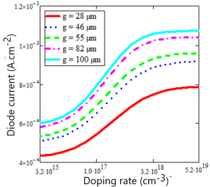
7.2. Influence of the Grain Size on the Effect of the Doping Rate on the Diode Current
To make an analysis of the impact of the grain size on the effect of the p-layer dopant concentration on the diode current, we simulated in
Figure 3 the diode current as a function of the impurity level for some crystal dimensions.
Figure 3. Diode current profile as a function of p-layer impurity for different crystal dimensions: Sfe = 103 cm/s, Sgs = 103 cm/s, Hb = 125 μm.
In
Figure 3, the diode current increases respectively with the dopant concentration and following crystal dimensions x and y. The increase of the photovoltage with the dopant concentration leads to an increase of losses in the transition zone (n+/p). The growth of these losses with large crystals is explained by the increase in the surfaces constituting the boundaries delimiting the crystal. On these surfaces reside defects of all kinds that lead to irregularities in the arrangement of the crystal lattice. These defects mainly arise from different treatments such as: grinding, polishing, chemical attack, coating with a layer of another substance. Examples of surface defects are: dangling bonds, micro cavities....
| [19] | A. Jakubowicz, (15 August 1985). «Theory of lifetime measurement with the scanning electron microscope in a semiconductor containing a localized defect: transient analysis». J. Appl. Phys. 58(4); pp 1483-1488. https://doi.org/10.1063/1.336080 |
[19]
.
We also find that, the diode current increases slightly with the size of the crystal for low dopant concentrations. Therefore, to minimize the losses in the n+/p transition zone, the concentration of the dopant must be between 1015cm
-3 and 1017cm
-3 for polycrystallines. And if the concentration of the dopant is greater than 1017cm
-3, weak grains should be used. Because in
Figure 3 when the doping rate is greater than 1017cm
-3, the diode current increases sharply as we increase the size of the crystal.
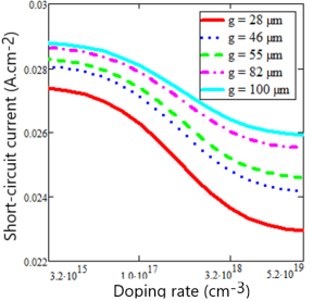
7.3. Influence of the Following Dimensions X and Y on the Effect of Doping Rate on Short Circuit Current
The short-circuit state is an operating point that allows us to characterize the energy performance of the solar cell. In any case, it is influenced by the dopant concentration of the p-layer, the crystal dimensions, etc.
Figure 4 allows for analyzing the impact of the crystal dimensions on the effect of the doping rate on the short-circuit current.
Figure 4. Short-circuit current profile as a function of the p-layer dopant for different crystal dimensions: Sgs = 103 cm/s, Hb = 125 μm.
In
Figure 4, when Np 3.2.1015 cm-3, the short-circuit current decreases and this decrease is all the more slow than when the dimensions of the crystal are large. Deep energy levels in the bandgap are responsible for the drop in carrier lifetime with the dopant level, creating recombination centers according to
| [8] | Diallo, H. L., Seïdou Maiga, A., Wereme, A. and Sissoko, G. (2008) New Approach of Both Junction and Back Surface Recombination Velocities in a 3D Modelling Study of a Polycrystalline Silicon Solar Cell. The European Physical Journal Applied Phys ics, 42, 203-211. https://doi.org/10.1051/epjap:2008085 |
| [9] | Omar M., Thiame M., LY I., Datta I., Diouf M. S., Traore Y., Ndiaye M. and Sissoko G., (2016). 3D Study of a Polycrystalline Bifacial Silicon Solar Cell, Illuminated Simultaneously by Both Sides: Grain Size and Recombination Velocity Influence. International Journal of Innovative Science, Engineering & Technology, Vol. 3 Issue 12, pp. 152-162 http://www.ijiset.com |
[8, 9]
. Which leads to a reduction in the current of the circuit. And the increase in the dimensions of the crystal leads to a decrease in loss centers and the capture effect at the interfaces. Those that explain the decrease in the effect of the dopant level on the short-circuit current with the increase in crystal dimensions (following dimensions x and y). So to reduce the impact of p-layer dopant level on short circuit current, designers need to use large crystals.
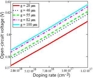
7.4. Influence of the Grain Size on the Effect of the Doping Rate on the Open-circuit Photovoltage
In this part, the influence of the grain size and the capture effect at the interface on the effect of the doping rate on the open-circuit voltage was studied.
Figure 5 highlights the impact of grain size and capture effect at interfaces on the effect of dopant on open-circuit voltage.
Figure 5. Profile of the open-circuit voltage as a function of the optimal p-layer dopant for different crystal dimensions: Scs = 103 cm/s, Hb = 125 μm.
In
Figure 5, we observe an increase in the circuit voltage-open with the x and y dimensions of the crystal and the dopant level of the layer P. The increase in the open circuit voltage with the dimensions of the crystal is more visible than with the optimal dopant levels of the layer P of the crystal. This is explained by: when these two parameters believe, there is a decrease in the diffusion coefficient and the lifetime of the carriers in the p layer.
Increasing the dopant concentration in the solar cell leads to an increase in losses in the n+/p transition region. This is due, on the one hand, to the increased density of minority carriers (electrons in the p region, holes in the n region) near the junction and, on the other, to the release of energy in the form of heat by the carriers instead of being collected as an electric current. So the higher the dopant concentration, the greater the probability of recombination. This leads to an increase in open-circuit voltage with increasing p-layer doping.
8. Conclusion
In this work, we focus on the choice of a polycrystalline silicon solar cell and the impact of its crystal size on the effect of p-layer doping. The choice is made with the aim of improving the performance of polycrystalline silicon solar celles and reducing losses.
Increasing the dopant concentration in the cell leads to higher losses in the n+/p transition zone. This leads to a reduction in effective diffusion length and short-circuit current on the one hand, and an increase in diode current and open-circuit voltage on the other.
Analysis of the effect of crystal size along the x and y axes shows that for p-layer impurity levels between 1015 and 1017 cm-3, doping losses decrease on these parameters, and these losses are greater than if crystal dimensions along x and y are small.
This shows that the effective diffusion length and short-circuit current decrease less with low p-layer doping rates when the following dimensions x and y are respected. Diode current, meanwhile, increases only slightly with subsequent crystal dimensions x and y in this p-layer doping range.
Abbreviations
Jsc | Circuit Current |
Voc | Open Circuit Voltage |
Sb | Back Surface Recombination Velocity |
Author Contributions
Moussa Camara: Conceptualization, Methodology, Validation, Writing – original draft, Writing – review & editing
Mamoudou Toure: Supervision
Haba Siba: Visualization
Hammady Cherif Diallo: Visualization
Moustapha Thiame: Supervision, Validation
Conflicts of Interest
There is no conflicts of interest.
References
| [1] |
Yong Zhao; Chunjun Liang; Mengjie Sun; Qian Liu; Fujun Zhang; Dan Li; Zhiqun He (2014) Effect of doping on the short-circuit current and open-circuit voltage of polymer solar cells. Appl. Phys. 116, 154506:
http://dx.doi.org/10.1063/1.4898692
|
| [2] |
Traore, S., Diedhiou, A., Sambou, A. and Camara, M. (2024) Study of the Electrical Parameters of a Silicon Solar Cell (n+/p/p+) under the Effect of Tempera ture by Optimization of the Base Thickness and the Doping Rate. Journal of Materials Science and Chemical Engineering, 12, 15-23.
https://doi.org/10.4236/msce.2024.1211002
|
| [3] |
Thiame, M., Camara, M., Lemrabott, H., Lemine Cheikh, M., Gueye, S. and Sissoko, G. (2023) Étude a 3d de la photopile au silicium polycristallin: Optimisation du taux de dopage en fonction de l’épaisseur de la base. International Journal of Advanced Research, 11, 311-322.
https://doi.org/10.21474/ijar01/17989
|
| [4] |
Sada Traore, Ansoumane Diedhiou and Momath Ndiaye (2024) Study of the performance parameters of a silicon solar cell (n+/p/p+) in frequency modulation placed in a medium dominated by the magnetic field: Effect of low and high doping rate Journal of Engineering and Technology Research Vol. 16(2), pp. 23-28
http://www.academicjournals.org/JETR
|
| [5] |
Camara, M., Ba, M. L., Diop, G., Ba, A. M., Diatta, I., Thiame, M., and Sissoko, G. (2020). 3D modelling study of silicon solar cell: effet of doping rate and grain Size, Journal of Scientific and Engineering, Research, 7(10), 14-24.
|
| [6] |
Ramatou Konate, Bernard Zouma, a), Mahamadi Savadogo, Fabe Idrissa Barro, Issa Zerbo, Martial Zoungrana, and Dieudonné Joseph Bathiebo (2023) Impacts of the Base and Emitter Doping Rate on the Internal Quantum Efficiency
https://doi.org/10.1063/5.0177051
|
| [7] |
F. I. Barro et al. (2015) “Theoretical investigation of base doping and illumination level effects on a bifacial silicon solar cell,” Br. J. Appl. Sci. Technol. 7(6), 610–618 (2015).
https://doi.org/10.9734/BJAST/2015/15628
|
| [8] |
Diallo, H. L., Seïdou Maiga, A., Wereme, A. and Sissoko, G. (2008) New Approach of Both Junction and Back Surface Recombination Velocities in a 3D Modelling Study of a Polycrystalline Silicon Solar Cell. The European Physical Journal Applied Phys ics, 42, 203-211.
https://doi.org/10.1051/epjap:2008085
|
| [9] |
Omar M., Thiame M., LY I., Datta I., Diouf M. S., Traore Y., Ndiaye M. and Sissoko G., (2016). 3D Study of a Polycrystalline Bifacial Silicon Solar Cell, Illuminated Simultaneously by Both Sides: Grain Size and Recombination Velocity Influence. International Journal of Innovative Science, Engineering & Technology, Vol. 3 Issue 12, pp. 152-162
http://www.ijiset.com
|
| [10] |
M. Thiame, A. Diene, B. Seibou, Cheick. Tidiane. Sarr, M. L. O. Cheikh, Ibrahima. Diatta, M. Dieye, Youssou. Traoré, Gregoire. Sissoko, (2017). 3D Study of a Bifacial Polycrystalline Silicon Solar Cell Back Surface Illuminated: Influence of Grain Size and Recombination Velocity, JSER. 4(1) pp 135-145.
|
| [11] |
Mountaga Boiro, Amadou Diao, Adama Ndiaye, Diène Gackou (2024) Influence of Wavelength on the Diffusion Capacitance of a Serial Vertical Junction Silicon Solar Cell in Frequency Regime American Journal of Materials Science and Engineering, 2024, Vol. 12, No. 2, 25-29 Available online at
http://pubs.sciepub.com/ajmse/12/2/1
|
| [12] |
Moussa Camara, Mamoudou Toure, Haba Siba, Mahamat Batran Mouta, Ousmane Fanta Camara and Moustapha Thiame (2025) Analyse of Impact of Temperature, Grain Size, and Magnetic Field on Effective Diffusion, Asian Journal of Science and Technology 16, (02), 13516-13519 at
http://www.journalajst.com
|
| [13] |
Moussa Camara, Moustapha Thiame, Mamoudou Touré, Haba Siba and Ousmane Fanta Camara 1 (2025) Effect of Crystal Size on the Optimum Temperature for the Highest Capacity of Tree-Dimensional Polycrystalline Silicon Solar Cell, Int. J. Adv. Res. 13(01), 443-452
https://dx.doi.org/10.21474/IJAR01/20215
|
| [14] |
Mayoro D., Senghane Mb, Martial Z., Issa Z., Biram D., Gregoire S. (2015) A 3D Modelling of Solar Cell’s Electric Power under Real Operating Point World Journal of Condensed Matter Physics, 2015, 5, 275-283
http://dx.doi.org/10.4236/wjcmp.2015.54028
|
| [15] |
Kosso AM. M., Thiame M., Youssou. T., Ibrahima D., Malick Nd., Lemrabott H., Ibrahima L., Gregoire. Sissoko, (2018). 3D Study of a Silicon Solar Cell under Constant Monochromatic Illumination: Influence of Both, Temperature and Magnetic Field. Journal of Scientific and Engineering Research, 5(7), pp. 259-269 online
http://www.jsaer.com
|
| [16] |
Ramatou K., Bernard Z., Adama O., Bruno K., Martial Z., Sié K (2022) Impact of the Thicknesses of the p and p+ Regions on the Electrical Parameters of a Bifacial PV Cell Energy and Power Engineering, 2022, 14, 133-145
https://www.scirp.org/journal/epe
|
| [17] |
Fabe. I. B et al. “On the capacitance of crystalline silicon solar cells in steady state,” Turk. J. Phys. 39, 122–127 (2015).
https://doi.org/10.3906/fiz-1408-3
|
| [18] |
J. Oualid, M. Bonfils, J. P. Crest, G. Mathian, H. Amzil, J. Dugas, M. Zehaf and S. Martinuzzi, (1982). «Photocurrent and Diffusion Lengths at the Vicinity of Grain Boundaries (g.b.) in N and P-type Polysilicon. Evaluation of the g.b. Recombination Velocity». Revue Phys. Appl. 17, pp. 119-124.
https://doi.org/10.1051/rphysap:01982001703011900
|
| [19] |
A. Jakubowicz, (15 August 1985). «Theory of lifetime measurement with the scanning electron microscope in a semiconductor containing a localized defect: transient analysis». J. Appl. Phys. 58(4); pp 1483-1488.
https://doi.org/10.1063/1.336080
|
Cite This Article
-
APA Style
Camara, M., Toure, M., Siba, H., Diallo, H. C., Camara, O. F., et al. (2025). Impact of Polycrystalline Crystal Size and the Capture Effect at the Contact Surface of Two Crystals on the Effect of P-layer Dopant on Some Electrical Parameters. International Journal of Sustainable and Green Energy, 14(3), 211-217. https://doi.org/10.11648/j.ijsge.20251403.17
 Copy
|
Copy
|
 Download
ACS Style
Camara, M.; Toure, M.; Siba, H.; Diallo, H. C.; Camara, O. F., et al. Impact of Polycrystalline Crystal Size and the Capture Effect at the Contact Surface of Two Crystals on the Effect of P-layer Dopant on Some Electrical Parameters. Int. J. Sustain. Green Energy 2025, 14(3), 211-217. doi: 10.11648/j.ijsge.20251403.17
Copy
|
Download
AMA Style
Camara M, Toure M, Siba H, Diallo HC, Camara OF, et al. Impact of Polycrystalline Crystal Size and the Capture Effect at the Contact Surface of Two Crystals on the Effect of P-layer Dopant on Some Electrical Parameters. Int J Sustain Green Energy. 2025;14(3):211-217. doi: 10.11648/j.ijsge.20251403.17
Copy
|
Download
-
@article{10.11648/j.ijsge.20251403.17,
  author = {Moussa Camara and Mamoudou Toure and Haba Siba and Hammady Cherif Diallo and Ousmane Fanta Camara and Moustapha Thiame},
  title = {Impact of Polycrystalline Crystal Size and the Capture Effect at the Contact Surface of Two Crystals on the Effect of P-layer Dopant on Some Electrical Parameters
},
  journal = {International Journal of Sustainable and Green Energy},
  volume = {14},
  number = {3},
  pages = {211-217},
  doi = {10.11648/j.ijsge.20251403.17},
  url = {https://doi.org/10.11648/j.ijsge.20251403.17},
  eprint = {https://article.sciencepublishinggroup.com/pdf/10.11648.j.ijsge.20251403.17},
  abstract = {Silicon ingots can be crystallized using a variety of processes. These lead to different qualities of crystal, and therefore of solar cell, depending on whether the silicon obtained is polycrystalline, i.e. made up of a multitude of crystals of varying size and orientation, or monocrystalline, i.e. formed from a single crystal. Like crystallization, doping is one of the steps in the silicon manufacturing process. Studying the doping level of a solar cell is crucial, as it has a direct influence on its performance, particularly its ability to convert sunlight into electricity. Doping, which consists in introducing impurities into silicon, modifies the electrical properties of the material and, consequently, the characteristics of the solar cell. The aim of this study is to assess the impact of polycrystalline crystal size and the capture effect at the contact surface of two crystals on the effect of p-layer dopant on effective diffusion length, diode current, short-circuit current and open-circuit voltage. Using the continuity equation with generation-recombination phenomena, this study found mathematical expressions for the fundamental electrical parameters needed to characterize solar cells. These mathematical expressions relate the effective diffusion length, diode current and electrical parameters such as short-circuit current and open-circuit voltage to the p-layer doping rate, crystal dimensions and carrier loss rate at the interfaces, respectively. Then, using Mathcad software, we simulated the impact of crystal size and the effect of captures at crystal interfaces on the influence of p-layer doping rate on effective diffusion length, diode current and electrical parameters such as Jsc and Voc. The results obtained from this analysis reveal that: For low values of p-layer doping rate and crystal size, the short-circuit current and effective diffusion length decrease less with low p-layer doping rates. On the other hand, for p-layer doping rates higher than 1017cm-3, the effective diffusion length and short-circuit current intensity decrease, but this decrease is faster when the crystal size is smaller. Diode current and open-circuit voltage increase with p-layer doping rate and crystal size. Growth is greatest when the p-layer doping rate is greater than 1017 cm-3 for diode current. The results of this study make it possible to design more efficient solar cells for polycrystalline silicon photovoltaic applications by keeping the doping rate at or below 1017 cm-3.
},
 year = {2025}
}
Copy
|
Download
-
TY  - JOUR
T1  - Impact of Polycrystalline Crystal Size and the Capture Effect at the Contact Surface of Two Crystals on the Effect of P-layer Dopant on Some Electrical Parameters

AU  - Moussa Camara
AU  - Mamoudou Toure
AU  - Haba Siba
AU  - Hammady Cherif Diallo
AU  - Ousmane Fanta Camara
AU  - Moustapha Thiame
Y1  - 2025/09/11
PY  - 2025
N1  - https://doi.org/10.11648/j.ijsge.20251403.17
DO  - 10.11648/j.ijsge.20251403.17
T2  - International Journal of Sustainable and Green Energy
JF  - International Journal of Sustainable and Green Energy
JO  - International Journal of Sustainable and Green Energy
SP  - 211
EP  - 217
PB  - Science Publishing Group
SN  - 2575-1549
UR  - https://doi.org/10.11648/j.ijsge.20251403.17
AB  - Silicon ingots can be crystallized using a variety of processes. These lead to different qualities of crystal, and therefore of solar cell, depending on whether the silicon obtained is polycrystalline, i.e. made up of a multitude of crystals of varying size and orientation, or monocrystalline, i.e. formed from a single crystal. Like crystallization, doping is one of the steps in the silicon manufacturing process. Studying the doping level of a solar cell is crucial, as it has a direct influence on its performance, particularly its ability to convert sunlight into electricity. Doping, which consists in introducing impurities into silicon, modifies the electrical properties of the material and, consequently, the characteristics of the solar cell. The aim of this study is to assess the impact of polycrystalline crystal size and the capture effect at the contact surface of two crystals on the effect of p-layer dopant on effective diffusion length, diode current, short-circuit current and open-circuit voltage. Using the continuity equation with generation-recombination phenomena, this study found mathematical expressions for the fundamental electrical parameters needed to characterize solar cells. These mathematical expressions relate the effective diffusion length, diode current and electrical parameters such as short-circuit current and open-circuit voltage to the p-layer doping rate, crystal dimensions and carrier loss rate at the interfaces, respectively. Then, using Mathcad software, we simulated the impact of crystal size and the effect of captures at crystal interfaces on the influence of p-layer doping rate on effective diffusion length, diode current and electrical parameters such as Jsc and Voc. The results obtained from this analysis reveal that: For low values of p-layer doping rate and crystal size, the short-circuit current and effective diffusion length decrease less with low p-layer doping rates. On the other hand, for p-layer doping rates higher than 1017cm-3, the effective diffusion length and short-circuit current intensity decrease, but this decrease is faster when the crystal size is smaller. Diode current and open-circuit voltage increase with p-layer doping rate and crystal size. Growth is greatest when the p-layer doping rate is greater than 1017 cm-3 for diode current. The results of this study make it possible to design more efficient solar cells for polycrystalline silicon photovoltaic applications by keeping the doping rate at or below 1017 cm-3.

VL  - 14
IS  - 3
ER  -
Copy
|
Download